

Global foundry capacity is not constrained uniformly. Demand, utilization, capital intensity, and profitability vary sharply across process nodes, creating very different investment profiles. Advanced logic and advanced packaging face persistent capacity pressure, while some mature digital nodes are experiencing increasing competition and pricing pressure. For investors and semiconductor companies, the opportunity lies in identifying where capacity remains structurally scarce and where new investment can generate defensible returns.
Foundry Capacity Is Fragmenting Across Process Nodes
Contract manufacturing spans several distinct technology categories. Leading-edge logic at 3nm and below serves AI accelerators, high-performance computing processors, and premium smartphone chips, requiring EUV lithography and extremely capital-intensive manufacturing infrastructure.
Mature and trailing nodes from approximately 28nm to 90nm and beyond support automotive microcontrollers, industrial sensors, connectivity devices, and display drivers. Specialty processes address applications requiring specific electrical characteristics, including BCD for power management, RF-SOI for radio-frequency applications, and SiC/GaN processes for high-voltage power conversion.
The supply-demand balance differs considerably between these categories. Advanced logic capacity remains heavily concentrated among a small number of foundries, while substantial additions to mature-node capacity, particularly in China, have increased the risk of localized oversupply and pricing pressure in standard digital CMOS.
Advanced Packaging Has Become a Critical Bottleneck
The growth of AI infrastructure is creating capacity pressure beyond wafer fabrication. Larger accelerator systems require increasingly sophisticated 2.5D and 3D packaging to integrate compute dies, HBM stacks, and high-speed interconnects.
TSMC’s CoWoS capacity has expanded rapidly, from approximately 35,000 wafers per month in late 2024 to around 75,000 in 2025, with the supplied research projecting 120,000 to 140,000 wafers per month by the end of 2026. Further expansion is planned toward approximately 260,000 wafers per month by the end of 2028 across facilities in Taiwan and Arizona.
Even with this expansion, the research estimates a potential 10% to 20% supply-demand gap through 2026–2027. This creates opportunities for alternative advanced-packaging providers, including ASE Technology Holding, Amkor, UMC, and Intel Foundry, particularly where customers need additional capacity or greater supply-chain diversification.
For companies evaluating these opportunities, a Foundry market assessment needs to distinguish between wafer-fabrication capacity and downstream packaging constraints. A shortage in one layer of the manufacturing chain can limit the commercial value of capacity added elsewhere.
Specialty Processes Can Offer More Defensible Economics
Mature-node investment is not inherently unattractive. The commercial case depends heavily on process specialization and customer concentration.
Automotive BCD processes, for example, integrate high-voltage power management, analog sensing, and digital logic. Specialized tooling and lengthy automotive qualification cycles can create barriers to entry that are absent in standard digital CMOS. These characteristics can protect specialized capacity from direct price competition.
Wide-bandgap power manufacturing presents another potential growth pool. The transition from 150mm to 200mm SiC wafers can reduce unit production costs by approximately 20% to 30% for manufacturers capable of achieving competitive crystal-growth and wafer-processing yields. Structural demand from EV powertrains, renewable energy, and other high-voltage applications provides a longer-term demand foundation.
The distinction is therefore between mature technology that is commoditized and mature technology that solves a specialized customer requirement. The latter can retain pricing power even when standard digital capacity is oversupplied.
Investment Economics Depend on Utilization and Customer Commitments
Fab construction involves substantial upfront capital, but utilization determines how effectively that investment is converted into revenue. A new facility entering an oversupplied node may struggle to recover depreciation and operating costs even if the initial construction economics appear attractive.
Customer commitments can materially reduce this risk. Multi-year offtake agreements, take-or-pay structures, and non-recurring engineering commitments can provide greater visibility into future wafer demand before capital is deployed.
A robust investment model should therefore compare projected demand with the global capacity pipeline rather than relying on current utilization alone. Announced fabs, equipment lead times, subsidy programs, customer commitments, power costs, and expected yield curves all influence the point at which additional capacity becomes economically justified.
Nexdigm Foundry Opportunity Assessment Framework
A structured assessment can screen new capacity investments through six decision gates:
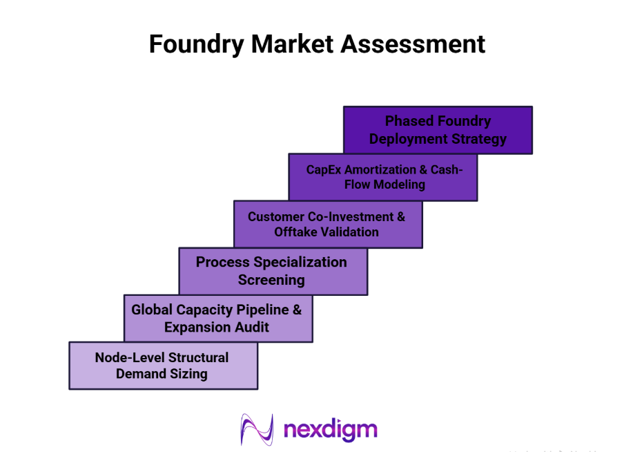
- Node-Level Structural Demand Sizing: Separate secular growth applications from cyclical demand and estimate wafer requirements by process technology.
- Global Capacity Pipeline & Expansion Audit: Track announced fabs, equipment deployment, construction timelines, and regional capacity additions.
- Process Specialization Screening: Compare specialty opportunities such as BCD, RF-SOI, SiC, and GaN with commoditized digital CMOS.
- Customer Co-Investment & Offtake Validation: Assess multi-year capacity commitments, take-or-pay agreements, design wins, and NRE contributions.
- CapEx Amortization & Cash-Flow Modeling: Model wafer costs, depreciation, utilities, yield ramp, and cash generation across different utilization scenarios.
- Phased Foundry Deployment Strategy: Determine whether advanced packaging, specialty conversion, or greenfield fabrication provides the strongest risk-adjusted entry point.
Nexdigm Case Study: Mapping Semiconductor Investment Opportunities in India
Nexdigm’s semiconductor and memory technology market assessment for India evaluated chip design houses, OEMs, packaging units, localization policies, data-center capacity expansion, and fabless ecosystem constraints across Bengaluru, Hyderabad, Gujarat, and Assam.
The assessment estimated India’s semiconductor market at $3.83 billion in 2024 and projected it to reach $12.13 billion by 2030, representing a 21.2% CAGR. It also identified strategic joint-venture and investment priorities alongside ecosystem bottlenecks, illustrating how market sizing, ecosystem mapping, and investment analysis can be combined to identify where additional semiconductor capacity is commercially relevant.
To take the next step, simply visit our Request a Consultation page and share your requirements with us.
Harsh Mittal
+91-8422857704