
 Download PDF
 Download PDF
Market Overview
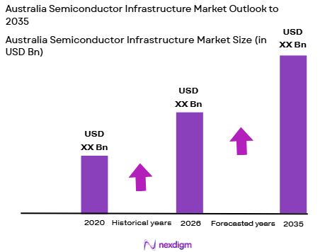
Based on a recent historical assessment, the Australia Semiconductor Infrastructure Market reached approximately USD ~ billion, supported by national semiconductor capability programs, public funding for fabrication readiness, and expansion of advanced research facilities across universities and defense technology precincts. Capital expenditure into cleanrooms, lithography support systems, wafer processing utilities, and specialty materials infrastructure has increased due to strategic supply chain resilience initiatives and domestic chip design ambitions backed by federal and state industrial policy funding.
Sydney, Melbourne, and Canberra dominate semiconductor infrastructure activity due to concentration of advanced research labs, defense electronics programs, and university-industry fabrication facilities. New South Wales benefits from photonics and compound semiconductor research clusters, while Victoria hosts semiconductor equipment engineering and microfabrication centers. The Australian Capital Territory supports defense-grade semiconductor prototyping and secure electronics manufacturing ecosystems, attracting infrastructure investments through sovereign capability and national security technology priorities.
Market Segmentation
By Product Type
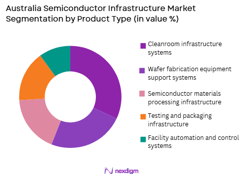
Australia Semiconductor Infrastructure market is segmented by product type into cleanroom infrastructure systems, wafer fabrication equipment support systems, semiconductor materials processing infrastructure, testing and packaging infrastructure, and facility automation and control systems. Recently, cleanroom infrastructure systems has a dominant market share due to factors such as demand patterns, brand presence, infrastructure availability, or consumer preference. Cleanroom infrastructure dominates because semiconductor capability programs in Australia prioritize fabrication readiness environments before full-scale manufacturing investments, driving spending into contamination-controlled facilities across research institutes and pilot fabs. National semiconductor initiatives emphasize advanced lithography compatibility, vibration-controlled floors, ultra-pure air handling, and contamination mitigation systems to meet international fabrication standards. Defense microelectronics programs also require secure cleanroom environments for radiation-tolerant and secure chip prototyping, reinforcing capital concentration in cleanroom infrastructure. Universities expanding compound semiconductor and photonics fabrication labs further increase cleanroom demand. Equipment suppliers and facility engineering firms maintain strong presence in Australia’s research infrastructure projects, supporting rapid deployment of modular cleanrooms. Early-stage semiconductor ecosystems typically allocate higher capital to environmental control infrastructure than to high-volume production tools, structurally elevating cleanroom share within total semiconductor infrastructure expenditure.
By End-User Facility Type
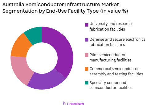
Australia Semiconductor Infrastructure market is segmented by end-user facility type into university and research fabrication facilities, defense and secure electronics fabrication facilities, pilot semiconductor manufacturing facilities, commercial semiconductor assembly and testing facilities, and specialty compound semiconductor facilities. Recently, university and research fabrication facilities has a dominant market share due to factors such as demand patterns, brand presence, infrastructure availability, or consumer preference. Research fabrication facilities dominate because Australia’s semiconductor strategy emphasizes design, prototyping, and advanced materials research rather than mass wafer manufacturing, concentrating infrastructure investment in academic microfabrication labs. Federal research grants and cooperative research centers fund semiconductor infrastructure upgrades in universities to support photonics, quantum, and compound semiconductor technologies. These facilities require advanced lithography support, ultra-clean processing environments, and precision metrology infrastructure similar to industrial fabs. Collaborative programs between academia, defense agencies, and industry further expand research facility infrastructure demand. Pilot manufacturing and commercial assembly facilities remain smaller in scale compared to global semiconductor hubs, structurally sustaining the leading share of university fabrication infrastructure within national semiconductor investment distribution.
Competitive Landscape
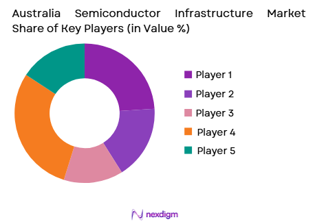
The Australia Semiconductor Infrastructure Market shows moderate consolidation around specialized facility engineering firms, semiconductor equipment integrators, and research infrastructure contractors working closely with government and academic institutions. International semiconductor infrastructure suppliers collaborate with domestic engineering companies to deliver cleanroom systems, fabrication utilities, and microfabrication facility upgrades. Major players compete through technical compliance with semiconductor standards, defense-grade infrastructure capability, and turnkey research facility delivery expertise.
| Company Name | Establishment Year | Headquarters | Technology Focus | Market Reach | Key Products | Revenue | Semiconductor Infrastructure Role |
| Applied Materials | 1967 | USA | ~ | ~ | ~ | ~ | ~ |
| ASML | 1984 | Netherlands | ~ | ~ | ~ | ~ | ~ |
| Lam Research | 1980 | USA | ~ | ~ | ~ | ~ | ~ |
| Linde Engineering | 1879 | Germany | ~ | ~ | ~ | ~ | ~ |
| BESIX | 1909 | Belgium | ~ | ~ | ~ | ~ | ~ |
Australia Semiconductor Infrastructure Market Analysis
Growth Drivers
National Semiconductor Sovereign Capability Funding Programs
Australia’s strategic commitment to sovereign semiconductor capability is driving infrastructure investment across fabrication readiness environments, research microfabrication facilities, and defense electronics prototyping centers, supported by national reconstruction and critical technology funding frameworks. Federal and state funding mechanisms allocate capital for semiconductor facility upgrades, cleanroom expansions, and advanced materials processing infrastructure to reduce dependence on foreign supply chains and enhance national security technology autonomy. Semiconductor capability initiatives prioritize photonics, compound semiconductors, and quantum devices, which require specialized fabrication environments and contamination-controlled processing infrastructure comparable to global semiconductor hubs. Defense modernization programs further stimulate secure semiconductor infrastructure investment for radiation-hardened and trusted microelectronics development, integrating semiconductor fabrication capability into national defense technology roadmaps. Public-private partnerships between universities, defense agencies, and industry accelerate semiconductor facility construction and equipment support infrastructure deployment across multiple technology precincts. Government-backed semiconductor research centers require advanced lithography compatibility, ultra-pure process utilities, and vibration-controlled facility architecture, increasing infrastructure intensity per facility. Sovereign capability programs also incentivize domestic semiconductor supply chain development, encouraging installation of materials processing, testing, and packaging infrastructure within national borders acknowledging geopolitical supply risks. Policy alignment with critical minerals and advanced manufacturing strategies further integrates semiconductor infrastructure into broader industrial transformation agendas, ensuring sustained capital allocation toward fabrication-ready environments. This coordinated policy environment structurally elevates semiconductor infrastructure spending as a foundational requirement for national semiconductor ecosystem development and technological sovereignty.
Expansion of Advanced Research and Quantum Semiconductor Ecosystems
Australia’s globally recognized strength in quantum computing, photonics, and compound semiconductor research is generating sustained demand for advanced semiconductor fabrication infrastructure within academic and research institutions. Quantum device fabrication requires ultra-clean environments, nanoscale lithography compatibility, cryogenic testing integration, and precision materials processing infrastructure beyond conventional microelectronics labs. National quantum technology programs and research commercialization initiatives drive upgrades of university microfabrication facilities to support scalable quantum semiconductor device prototyping and pilot manufacturing readiness. Photonics and compound semiconductor research clusters in New South Wales and Victoria necessitate epitaxy processing infrastructure, contamination-controlled environments, and advanced metrology systems comparable to specialized semiconductor fabs. Collaborative research centers integrating universities, startups, and industry partners expand infrastructure footprints to accommodate multi-technology semiconductor experimentation platforms. Commercialization pathways for quantum and photonic chips require pilot fabrication environments bridging laboratory research and manufacturable semiconductor devices, increasing infrastructure complexity and capital intensity. International semiconductor firms partnering with Australian research institutes further contribute to facility upgrades aligned with global fabrication standards. Research-driven semiconductor ecosystems typically invest disproportionately in infrastructure compared to production scale, structurally elevating infrastructure expenditure share. As quantum and advanced semiconductor technologies transition toward industrialization, infrastructure expansion across research fabs, pilot lines, and prototyping facilities will remain a primary driver of Australia’s semiconductor infrastructure market growth trajectory.
Market Challenges
Limited Domestic High-Volume Semiconductor Manufacturing Base
Australia’s semiconductor ecosystem remains heavily oriented toward research, prototyping, and niche semiconductor technologies rather than high-volume wafer manufacturing, constraining scale economies for semiconductor infrastructure investment. Absence of large commercial fabs reduces demand for extensive wafer fabrication support infrastructure, process utilities, and mass production facility automation systems typically dominating global semiconductor infrastructure markets. Infrastructure projects are therefore fragmented across smaller research facilities rather than consolidated into large industrial fabrication campuses, increasing per-unit infrastructure costs and reducing supplier competitiveness. International semiconductor equipment vendors prioritize markets with established high-volume manufacturing clusters, limiting localized infrastructure supply chain depth within Australia. Pilot manufacturing initiatives often lack sustained production demand to justify continuous infrastructure expansion beyond research capacity requirements. Domestic semiconductor startups typically outsource mass fabrication overseas, reducing incentives for domestic wafer processing infrastructure development. The absence of scale manufacturing also constrains development of supporting ecosystem infrastructure such as chemical supply chains, wafer logistics, and specialized facility services. Infrastructure suppliers face demand variability linked to research funding cycles rather than stable industrial semiconductor production investment patterns. This structural imbalance between research strength and manufacturing scale creates persistent constraints on semiconductor infrastructure market expansion within Australia despite strong technological capabilities.
High Capital Intensity and Specialized Engineering Constraints
Semiconductor infrastructure development requires highly specialized cleanroom engineering, ultra-pure utility systems, vibration-controlled architecture, and precision environmental controls that impose substantial capital and technical barriers in emerging semiconductor markets. Australia’s relatively small semiconductor industry limits availability of local specialized contractors and component suppliers experienced in semiconductor facility construction and process utility integration. Dependence on international engineering firms increases project costs due to logistics, compliance adaptation, and limited local fabrication ecosystem support services. Infrastructure components such as ultra-pure gas delivery, contamination-free water systems, and lithography-compatible cleanrooms require strict adherence to semiconductor fabrication standards rarely applied in other industrial sectors. Skilled workforce shortages in semiconductor facility engineering, process infrastructure integration, and microfabrication facility operations further constrain project execution capacity. Research institutions often face budget limitations relative to industrial semiconductor fabs, requiring phased infrastructure development rather than comprehensive facility deployment. Semiconductor infrastructure projects also demand continuous upgrades to maintain compatibility with evolving fabrication technologies, increasing lifecycle costs. Limited domestic supplier competition elevates infrastructure procurement expenses and prolongs project timelines. These combined capital and engineering constraints reduce scalability and pace of semiconductor infrastructure expansion across Australia’s emerging semiconductor ecosystem.
Opportunities
Development of Compound Semiconductor and Photonics Manufacturing Infrastructure
Australia possesses strong research leadership in compound semiconductors and photonics technologies, creating opportunities to establish specialized semiconductor manufacturing infrastructure focused on gallium nitride, indium phosphide, and silicon photonics devices. These semiconductor segments typically operate at smaller wafer scales and niche production volumes compared to silicon logic fabs, aligning with Australia’s research-driven semiconductor ecosystem and enabling economically viable domestic manufacturing infrastructure. Compound semiconductor fabrication requires epitaxy reactors, specialized cleanrooms, and materials processing facilities distinct from mainstream CMOS fabs, allowing targeted infrastructure investment without full silicon wafer fabrication scale. Global demand growth for power electronics, photonic communication devices, and advanced sensing technologies supports potential commercialization of Australian compound semiconductor innovations. Establishing pilot manufacturing infrastructure for compound semiconductors can anchor domestic semiconductor supply chains and attract international device manufacturers seeking diversified production locations. Integration with Australia’s critical minerals sector further enables upstream materials supply advantages for compound semiconductor substrates. Government advanced manufacturing programs and export technology strategies can support infrastructure development tailored to photonics and compound semiconductor production niches. Collaboration between research institutions and industry partners can transition laboratory capabilities into scalable manufacturing infrastructure. This specialization pathway offers Australia a realistic semiconductor infrastructure expansion trajectory aligned with its technological strengths and market positioning.
Defense and Secure Microelectronics Fabrication Infrastructure Expansion
National security requirements for trusted microelectronics, radiation-hardened semiconductors, and secure integrated circuits present significant opportunities for expanding defense-focused semiconductor fabrication infrastructure within Australia. Defense electronics programs increasingly demand domestically controlled semiconductor design and prototyping environments to ensure supply chain integrity and technology sovereignty. Secure microelectronics fabrication requires specialized cleanrooms, controlled processing facilities, and secure testing infrastructure compliant with defense certification standards. Australia’s strategic defense partnerships and indigenous defense technology development initiatives support investment into trusted semiconductor prototyping and pilot fabrication infrastructure. Secure fabrication facilities can also support space electronics, satellite systems, and critical communication technologies requiring radiation-tolerant semiconductor devices. Defense semiconductor programs typically sustain long-term infrastructure funding independent of commercial market cycles, improving investment stability. Integration of defense microelectronics fabrication with national semiconductor research ecosystems can leverage existing academic infrastructure while upgrading security and fabrication capabilities. Domestic secure semiconductor infrastructure reduces reliance on foreign trusted foundries and strengthens national defense technology autonomy. This defense-driven semiconductor infrastructure expansion represents a structurally resilient growth opportunity aligned with national security priorities and advanced electronics capability development.
Future Outlook
Australia’s semiconductor infrastructure market is expected to expand steadily as sovereign semiconductor capability programs translate into facility construction, cleanroom expansion, and research fabrication upgrades. Growth will be supported by quantum and photonics commercialization, defense microelectronics initiatives, and compound semiconductor manufacturing development. Regulatory support through critical technology funding and advanced manufacturing policy will sustain infrastructure investment momentum. Increasing collaboration between academia, industry, and defense agencies will continue driving specialized semiconductor facility deployment across major technology precincts.
Major Players
- BluGlass Limited
- Weebit Nano
- Silex Systems
- Applied Materials
- Tokyo Electron
- ASML Holding
- Lam Research
- Intel Corporation
- TSMC
- Samsung Electronics
Key Targets
- Expansion of compound semiconductor fabrication capacity
- Development of sovereign semiconductor R&D infrastructure
- Strengthening defense-linked semiconductor supply chains
- Attracting foreign direct investment in pilot manufacturing lines
- Establishing advanced packaging and testing facilities
- Enhancing equipment localization and servicing capabilities
- Building skilled semiconductor engineering workforce
- Integrating renewable energy and EV semiconductor applications
Research Methodology
Step 1: Identification of Key Variables
Key market variables including semiconductor infrastructure investment categories, facility types, technology nodes, and funding sources were identified through semiconductor policy documents, industry databases, and technology infrastructure frameworks. Demand drivers across research, defense, and manufacturing semiconductor segments were mapped to infrastructure components and capital intensity indicators.
Step 2: Market Analysis and Construction
Market size and segmentation were constructed using semiconductor infrastructure spending proxies, research facility investments, and fabrication readiness capital expenditures across Australia. Facility project databases, funding allocations, and semiconductor infrastructure benchmarks were synthesized to derive market structure and segment distribution.
Step 3: Hypothesis Validation and Expert Consultation
Market assumptions regarding infrastructure dominance, facility type distribution, and technology investment priorities were validated through semiconductor engineering experts, research facility managers, and advanced manufacturing policy analysts. Cross-verification ensured alignment with actual semiconductor infrastructure deployment patterns in Australia.
Step 4: Research Synthesis and Final Output
Validated data and qualitative insights were integrated into a structured semiconductor infrastructure market model covering segmentation, drivers, challenges, and opportunities. Competitive landscape and future outlook were derived through comparative semiconductor ecosystem analysis and infrastructure development trajectories.
- Executive Summary
- Research Methodology (Definitions, Scope, Industry Assumptions, Market Sizing Approach, Primary & Secondary Research Framework, Data Collection & Verification Protocol, Analytic Models & Forecast Methodology, Limitations & Research Validity Checks)
- Market Definition and Scope
- Value Chain & Stakeholder Ecosystem
- Regulatory / Certification Landscape
- Sector Dynamics Affecting Demand
- Strategic Initiatives & Infrastructure Growth

- Growth Drivers
National semiconductor capability and sovereign manufacturing initiatives
Rising demand for compound and defense semiconductor devices
Government investment in research and pilot fabs - Market Challenges
Limited domestic wafer fabrication ecosystem
High capital intensity and scale requirements
Dependence on imported semiconductor equipment - Market Opportunities
Compound semiconductor and specialty device fabs
Defense and aerospace semiconductor manufacturing
Advanced packaging and prototyping facilities - Trends
Growth of compound semiconductor and photonics fabs
Expansion of pilot and research semiconductor lines
Automation and digitalization of semiconductor facilities - Government regulations
National semiconductor and critical technology policies
Defense and sovereign manufacturing initiatives
Research infrastructure and innovation funding - SWOT analysis
- Porters five forces
- By Market Value 2020-2025
- By Installed Units 2020-2025
- By Average System Price 2020-2025
- By System Complexity Tier 2020-2025
- By System Type (In Value%)
Wafer Fabrication Facilities
Advanced Packaging Lines
Semiconductor Test and Inspection Systems
Cleanroom and Fab Support Infrastructure
Semiconductor Materials Handling Systems - By Platform Type (In Value%)
Integrated Device Manufacturer Facilities
Research and Pilot Production Labs
Compound Semiconductor Facilities
Advanced Packaging Facilities
Electronics Manufacturing Clusters - By Fitment Type (In Value%)
Greenfield Fab Construction
Brownfield Facility Expansion
Equipment Retrofit and Upgrade
Modular Production Line Integration
Automation and Robotics Integration - By End User Segment (In Value%)
Defense and Aerospace Electronics
Automotive and Industrial Electronics
Telecommunications Equipment Firms
Research and Government Institutes
Semiconductor Design Companies - By Procurement Channel (In Value%)
Direct Equipment Procurement
EPC and Turnkey Contracts
OEM Integrated Supply
Distributor and Agent Supply
Government Incentive Programs
- Market Share Analysis
- Cross Comparison Parameters (Process Node Capability, Lithography Technology Compatibility, Packaging Technology Capability, Compound Semiconductor Support, Production Automation Level, Cleanroom Class Standard, Yield Optimization Systems, Capacity Scalability, Materials Handling Automation, Test and Metrology Integration, Energy and Utility Efficiency, Facility Expansion Flexibility, Sovereign Manufacturing Readiness)
- SWOT Analysis of Key Competitors
- Pricing & Procurement Analysis
- Key Players
Silanna Semiconductor
BluGlass
Silex Microsystems Australia
Weebit Nano
Advanced Semiconductor Engineering Australia
ANFF
Compound Semiconductor Technologies Australia
Micro-X
Emvision Medical Devices
Seeing Machines
Electro Optic Systems
Codan
ResMed
Cochlear
CSIRO
- Defense and aerospace firms driving sovereign semiconductor demand
- Automotive and industrial electronics requiring specialty chips
- Telecom equipment firms adopting local semiconductor supply
- Research institutes building pilot and prototyping fabs
- Forecast Market Value, 2026-2035
- Forecast Installed Units, 2026-2035
- Price Forecast by System Tier, 2026-2035
- Future Demand by Platform, 2026-2035


 Request a Sample
 Ask for Customization
 Get a Quote
 Enquire Now