
 Download PDF
 Download PDF
Market Overview
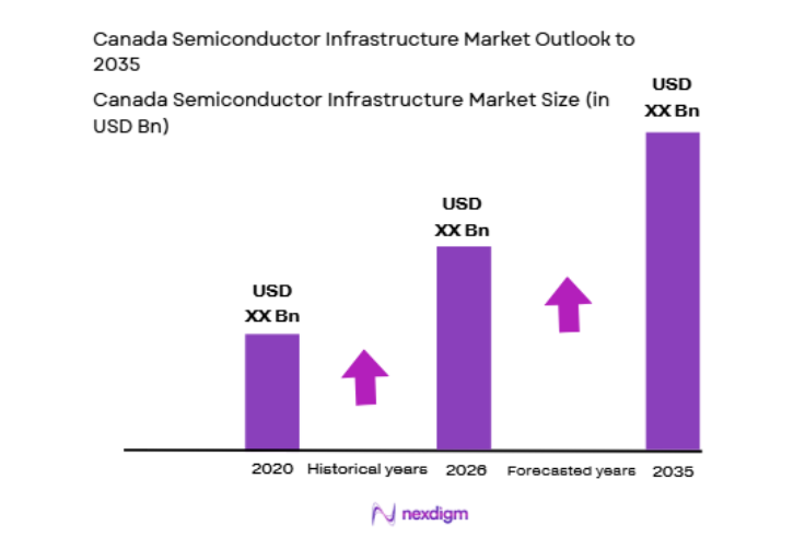
Canada semiconductor infrastructure market reached approximately USD ~ billion in semiconductor facility construction, cleanroom systems, and fabrication utilities investment based on a recent historical assessment, driven by national semiconductor supply chain resilience initiatives, photonics and compound semiconductor manufacturing programs, and North American electronics localization strategies. Infrastructure demand is expanding across wafer fabrication pilot lines, advanced packaging facilities, and semiconductor materials processing infrastructure supported by federal industrial innovation funding and private semiconductor manufacturing investments.
Toronto, Ottawa, and Montreal dominate Canada semiconductor infrastructure development due to semiconductor research institutes, photonics manufacturing clusters, and proximity to electronics and defense supply chains. Ottawa hosts compound semiconductor and photonics fabrication facilities, Montreal concentrates semiconductor research infrastructure and microelectronics institutes, while Toronto leads industrial engineering capacity and electronics manufacturing integration supporting semiconductor facility construction and packaging infrastructure deployment across Canada.
Market Segmentation
By Product Type
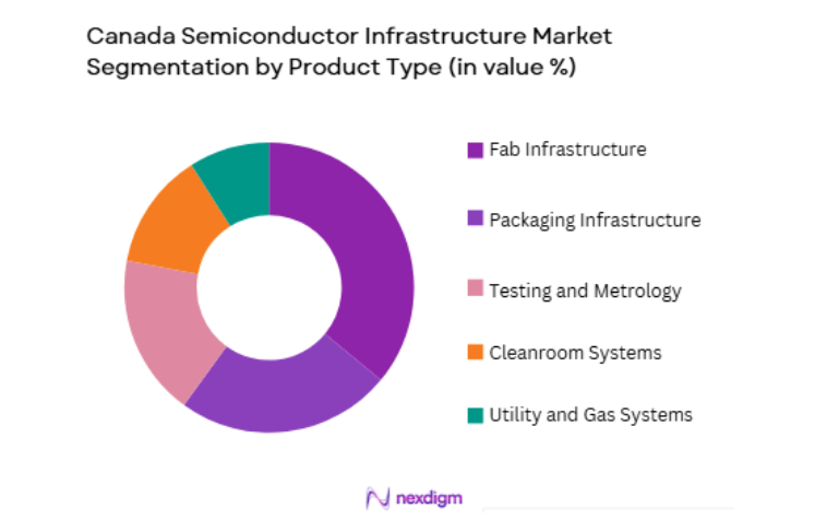
Canada Semiconductor Infrastructure market is segmented by product type into wafer fabrication facility infrastructure, assembly and packaging infrastructure, semiconductor testing and metrology infrastructure, cleanroom and contamination control systems, and semiconductor utility and gas delivery systems. Recently, wafer fabrication facility infrastructure has a dominant market share due to factors such as national semiconductor manufacturing capability programs, compound semiconductor fab development, and pilot fabrication line expansion across Canadian photonics and microelectronics clusters. Federal innovation funding prioritizes front-end manufacturing infrastructure to strengthen domestic semiconductor capability, resulting in higher capital allocation toward fabrication cleanrooms, utilities, and process systems compared with downstream packaging or testing segments.
By Platform Type
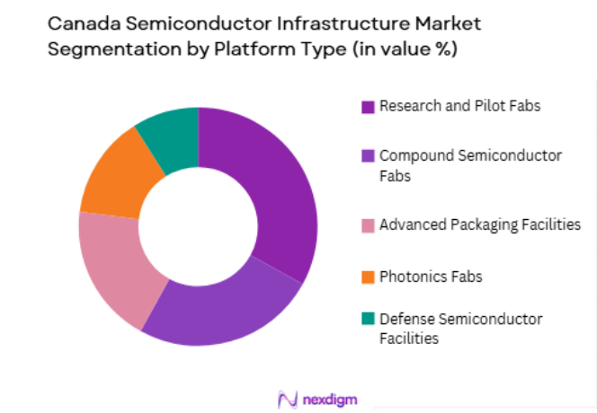
Canada Semiconductor Infrastructure market is segmented by platform type into research and pilot fabrication facilities, compound semiconductor manufacturing facilities, advanced packaging and assembly facilities, photonics fabrication facilities, and defense semiconductor facilities. Recently, research and pilot fabrication facilities has a dominant market share due to factors such as strong national semiconductor research ecosystem, public funding for microelectronics pilot lines, and technology transfer infrastructure supporting commercialization. Canada’s semiconductor strategy emphasizes research-to-manufacturing pathways, resulting in concentration of infrastructure spending in pilot fabs and prototyping facilities across universities, national labs, and innovation centers compared with large-scale commercial fabrication platforms.
Competitive Landscape
Canada semiconductor infrastructure market exhibits moderate consolidation, with global semiconductor facility engineering firms and domestic industrial construction companies collaborating on fabrication and packaging projects, while specialized cleanroom and process utility providers supply semiconductor-grade infrastructure systems. Major players leverage semiconductor EPC expertise, photonics facility experience, and North American industrial construction capabilities to secure research fab and compound semiconductor manufacturing infrastructure projects across Canada.
| Company Name | Establishment Year | Headquarters | Technology Focus | Market Reach | Key Products | Revenue | Semiconductor Facility Expertise |
| Exyte | 1912 | Germany | ~ | ~ | ~ | ~ | ~ |
| PCL Construction | 1906 | Canada | ~ | ~ | ~ | ~ | ~ |
| EllisDon | 1951 | Canada | ~ | ~ | ~ | ~ | ~ |
| Jacobs Solutions | 1947 | USA | ~ | ~ | ~ | ~ | ~ |
| Stantec | 1954 | Canada | ~ | ~ | ~ | ~ | ~ |
Canada Semiconductor Infrastructure Market Analysis
Growth Drivers
National Semiconductor and Photonics Manufacturing Capability Programs
Canada semiconductor infrastructure demand is strongly driven by federal and provincial programs aimed at establishing domestic semiconductor and photonics manufacturing capability to support strategic industries including telecommunications, defense, and advanced electronics. Government funding initiatives promote construction of pilot fabrication facilities, compound semiconductor fabs, and advanced packaging centers across research and industrial clusters, significantly increasing infrastructure investment. Canada’s strength in photonics and compound semiconductor research creates demand for specialized fabrication environments requiring cleanrooms, epitaxy systems, and semiconductor utilities infrastructure. Public funding reduces capital barriers for facility construction, enabling commercialization pathways from research to manufacturing. North American supply chain resilience initiatives encourage domestic semiconductor production capacity within allied economies, positioning Canada as a niche manufacturing location. Infrastructure projects generate regional high-technology employment and innovation capacity, aligning with national industrial policy priorities. Collaboration between universities, startups, and semiconductor firms drives facility expansion in research hubs.
North American Electronics and Defense Supply Chain Localization
Canada semiconductor infrastructure expansion is supported by localization of electronics and defense semiconductor supply chains within North America, driven by geopolitical resilience strategies and regional manufacturing integration across Canada and the United States. Defense and aerospace electronics systems increasingly require trusted domestic semiconductor fabrication and packaging capabilities, stimulating infrastructure investment in secure facilities. Canadian electronics manufacturers seek geographically proximate semiconductor sources to reduce import dependency and logistics risk, encouraging domestic facility development. Bilateral industrial cooperation programs support semiconductor capability within Canada as part of continental supply chain security. Infrastructure demand arises from specialized semiconductor applications such as RF, photonics, and power electronics used in defense and communications equipment. Localization initiatives prioritize secure fabrication and testing environments meeting defense standards, increasing facility complexity and capital intensity. Regional industrial clusters around Ottawa and Montreal support semiconductor manufacturing ecosystems. These factors collectively drive infrastructure expansion aligned with strategic supply chain objectives.
Market Challenges
Limited Scale of Commercial Semiconductor Manufacturing Ecosystem
Canada semiconductor infrastructure development faces structural limitations due to the relatively small scale of commercial semiconductor manufacturing activity compared with major global fabrication hubs, which constrains demand for large-scale fabrication facilities and reduces economies of scale for infrastructure investment. Most Canadian semiconductor activity is concentrated in research, prototyping, and niche compound semiconductor production rather than high-volume silicon manufacturing, limiting need for mega-fab infrastructure. Absence of leading-edge silicon wafer fabrication reduces attraction of global semiconductor manufacturers to establish large plants in Canada. Smaller domestic semiconductor firms often lack capital for commercial-scale facility construction. Infrastructure projects are therefore fragmented across research and pilot facilities rather than consolidated large fabs. Supply chain and equipment ecosystems remain underdeveloped relative to major semiconductor regions. Limited domestic demand reduces private sector incentives for infrastructure expansion. These factors collectively restrict large-scale semiconductor infrastructure growth.
Dependence on Imported Semiconductor Equipment and Process Technology
Canada semiconductor infrastructure projects rely heavily on imported semiconductor manufacturing equipment, process technology, and specialized materials from global suppliers, increasing cost, project complexity, and vulnerability to external supply constraints. Semiconductor fabs require advanced lithography, deposition, and metrology systems not produced domestically. Infrastructure design must align with foreign equipment specifications and standards. Import logistics and procurement lead times extend facility commissioning schedules. Export controls and supply chain disruptions can delay equipment delivery. Domestic workforce expertise in advanced semiconductor process integration remains limited. Infrastructure contractors depend on international technology partners. Currency fluctuations increase project costs. These dependencies constrain autonomous semiconductor infrastructure expansion in Canada.
Opportunities
Expansion of Compound Semiconductor and Photonics Manufacturing Clusters
Canada has significant opportunity to expand semiconductor infrastructure through development of compound semiconductor and photonics manufacturing clusters leveraging national research strengths and global demand growth in optical communications, sensing, and power electronics. Compound semiconductor fabrication requires specialized cleanroom and epitaxy infrastructure distinct from silicon fabs, creating targeted facility investment demand. Canadian photonics institutes provide commercialization pathways into manufacturing. Government innovation funding supports cluster-based facility development. Global semiconductor firms seek niche manufacturing partnerships. Photonics demand from telecom and defense sectors sustains infrastructure growth. Smaller fab scale reduces capital barriers relative to silicon mega-fabs. These clusters can position Canada as a specialized semiconductor manufacturing hub.
Advanced Packaging and Heterogeneous Integration Facility Development
Canada semiconductor infrastructure market can grow through expansion of advanced packaging and heterogeneous integration facilities supporting chiplet architectures and system-in-package technologies increasingly required in electronics and AI hardware. Advanced packaging requires precision assembly cleanrooms, bonding equipment infrastructure, and thermal management systems. Canada’s electronics manufacturing sector can integrate packaging capability with design and assembly. Packaging plants require lower capital than wafer fabs, enabling feasible domestic investment. North American semiconductor supply chain strategies emphasize packaging localization. Demand from AI and photonics devices supports packaging infrastructure growth. Collaboration with global semiconductor firms can establish packaging centers. This opportunity expands downstream semiconductor manufacturing infrastructure in Canada.
Future Outlook
Canada semiconductor infrastructure market is expected to expand steadily over the next five years as national semiconductor capability programs, photonics manufacturing initiatives, and North American supply chain localization policies translate into pilot fab, compound semiconductor, and advanced packaging facility construction. Continued government funding, defense electronics demand, and commercialization of semiconductor research will sustain infrastructure investment, strengthening Canada’s position in specialized semiconductor manufacturing segments.
Major Players
- Exyte
- PCL Construction
- EllisDon
- Jacobs Solutions
- Stantec
- Fluor Corporation
- AECOM
- WSP Global
- M+W Group
- Arup
- HDR Inc.
- Black & McDonald
- Bird Construction
- SNC-Lavalin
- Graham Construction
Key Target Audience
- Semiconductor manufacturers
- Photonics device companies
- Electronics manufacturers
- Defense electronics contractors
- Investments and venture capitalist firms
- Government and regulatory bodies
- Industrial infrastructure developers
- Semiconductor equipment suppliers
Research Methodology
Step 1: Identification of Key Variables
Semiconductor facility investment, pilot fab construction, photonics manufacturing infrastructure, and packaging facility deployment indicators were identified from industry and government funding disclosures. Key variables included cleanroom capacity, fabrication line installations, and semiconductor utility infrastructure development across Canada.
Step 2: Market Analysis and Construction
Canada semiconductor infrastructure market size was constructed using facility construction spending, semiconductor infrastructure contracts, and fabrication and packaging facility investments across research, photonics, and manufacturing clusters. Platform deployment patterns were mapped to infrastructure demand segments.
Step 3: Hypothesis Validation and Expert Consultation
Infrastructure demand assumptions were validated through consultation with semiconductor facility engineers, photonics manufacturing experts, and industrial construction specialists in Canada. Policy and supply chain drivers were cross-checked with national semiconductor strategy sources.
Step 4: Research Synthesis and Final Output
All quantitative and qualitative findings were synthesized into structured analysis covering segmentation, competitive landscape, growth drivers, and outlook. Data triangulation ensured consistency across infrastructure investment estimates and sector trends.
- Executive Summary
- Research Methodology (Definitions, Scope, Industry Assumptions, Market Sizing Approach, Primary & Secondary Research Framework, Data Collection & Verification Protocol, Analytic Models & Forecast Methodology, Limitations & Research Validity Checks)
- Market Definition and Scope
- Value Chain & Stakeholder Ecosystem
- Regulatory / Certification Landscape
- Sector Dynamics Affecting Demand

- Growth Drivers
National initiatives to develop domestic semiconductor manufacturing capability
Rising demand for chips in AI automotive and communications sectors
Expansion of research and specialty semiconductor fabrication facilities - Market Challenges
High capital intensity and long timelines of fab infrastructure projects
Dependence on imported semiconductor manufacturing equipment
Limited domestic advanced node manufacturing ecosystem - Market Opportunities
Development of specialty and compound semiconductor fabs in Canada
Expansion of semiconductor R and D and pilot fabrication lines
Growth of advanced packaging and OSAT infrastructure - Trends
Shift toward advanced packaging and heterogeneous integration facilities
Increasing automation and smart fab infrastructure adoption
Focus on energy efficient and sustainable semiconductor fabs - Government regulations
Canadian semiconductor and critical technology investment policies
Export control and technology transfer regulations
Environmental and facility compliance standards for fabs - SWOT analysis
- Porters Five forces
- By Market Value, 2020-2025
- By Installed Units, 2020-2025
- By Average System Price, 2020-2025
- By System Complexity Tier, 2020-2025
- By System Type (In Value%)
Wafer Fabrication Equipment Infrastructure
Assembly and Packaging Infrastructure
Semiconductor Materials Processing Infrastructure
Testing and Metrology Infrastructure
Cleanroom and Facility Systems - By Platform Type (In Value%)
Integrated Device Manufacturer Facilities
Foundry Manufacturing Facilities
OSAT and Packaging Facilities
Research and Pilot Fabrication Lines
Specialty Semiconductor Production Sites - By Fitment Type (In Value%)
Greenfield Fab Construction
Brownfield Fab Expansion
Modular Cleanroom Installations
Tool Level Infrastructure Integration
Utility and Facility Retrofits - By End User Segment (In Value%)
Integrated Device Manufacturers
Fabless Semiconductor Firms
Outsourced Assembly and Test Providers
- Market Share Analysis
- Cross Comparison Parameters (Process Node Capability, Fab Capacity, Packaging Technology, Facility Automation, Utility Efficiency, Cleanroom Class, Tool Integration Level, Yield Optimization Capability, Energy Consumption, Technology Specialization)
- SWOT Analysis of Key Competitors
- Pricing & Procurement Analysis
- Key Players
Applied Materials
ASML
Lam Research
KLA Corporation
Tokyo Electron
ASM International
Advantest
Teradyne
BE Semiconductor Industries
Kulicke and Soffa
Aixtron
Veeco Instruments
Edwards Vacuum
MKS Instruments
ULVAC
- IDMs investing in domestic specialty semiconductor capacity
- Fabless firms supporting local prototyping and pilot fabs
- OSAT providers expanding advanced packaging capabilities
- Research institutes developing semiconductor innovation facilities
- Forecast Market Value, 2026-2035
- Forecast Installed Units, 2026-2035
- Price Forecast by System Tier, 2026-2035
- Future Demand by Platform, 2026-2035


 Request a Sample
 Ask for Customization
 Get a Quote
 Enquire Now