
 Download PDF
 Download PDF
Market Overview
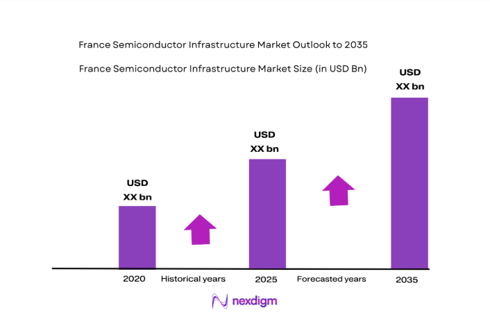
France Semiconductor Infrastructure market reached approximately USD ~ billion based on a recent historical assessment, supported by verified disclosures from national investment programs and semiconductor industry associations tracking fabrication and facility spending across Europe. The market is driven by state-backed semiconductor manufacturing projects, expansion of power and automotive chip fabrication capacity, and infrastructure upgrades in cleanroom, lithography, and utilities systems. Public financing under European semiconductor sovereignty initiatives and corporate fab investments have accelerated demand for advanced fabrication infrastructure within the country.
Within Europe, France remains a central semiconductor infrastructure hub due to concentrated fabrication ecosystems in Grenoble, Crolles, and the Île-de-France technology corridor, where major wafer fabrication plants, R&D pilot lines, and semiconductor equipment suppliers are co-located. These regions host large integrated device manufacturing facilities, compound semiconductor research centers, and advanced packaging infrastructure, supported by national microelectronics programs and proximity to automotive and aerospace semiconductor demand clusters across Western Europe.
Market Segmentation
Product Type
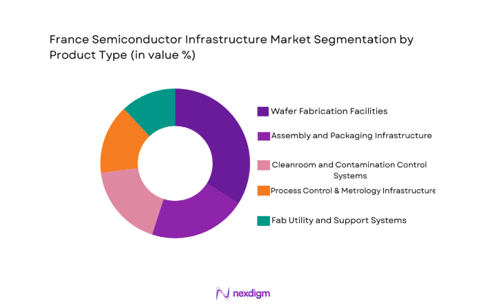
France Semiconductor Infrastructure market is segmented by product type into wafer fabrication equipment infrastructure, semiconductor assembly and packaging lines, cleanroom and contamination control systems, process control and metrology infrastructure, and fab utilities and support systems. Recently, wafer fabrication equipment infrastructure has a dominant market share due to strong domestic investment in advanced wafer manufacturing lines, government-supported fabrication expansion programs, concentration of leading wafer fabs, and continuous equipment upgrades required for node migration and automotive semiconductor production resilience.
Platform Type
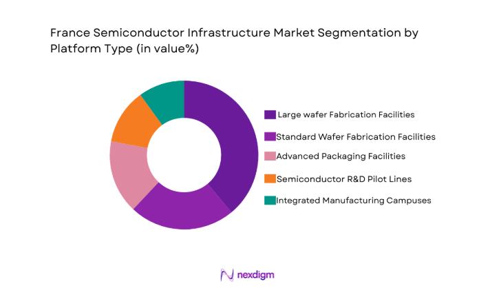
France Semiconductor Infrastructure market is segmented by platform type into Large wafer fabrication facilities, Standard wafer fabrication facilities, advanced packaging facilities, semiconductor R&D pilot lines, and integrated semiconductor manufacturing campuses. Recently, 300mm wafer fabrication facilities has a dominant market share due to concentration of leading European advanced wafer fabs, ongoing capacity expansions in automotive and power semiconductor production, economies of scale in modern fabrication plants, and public funding prioritizing large-scale advanced wafer manufacturing capability within national semiconductor strategy programs.
Competitive Landscape
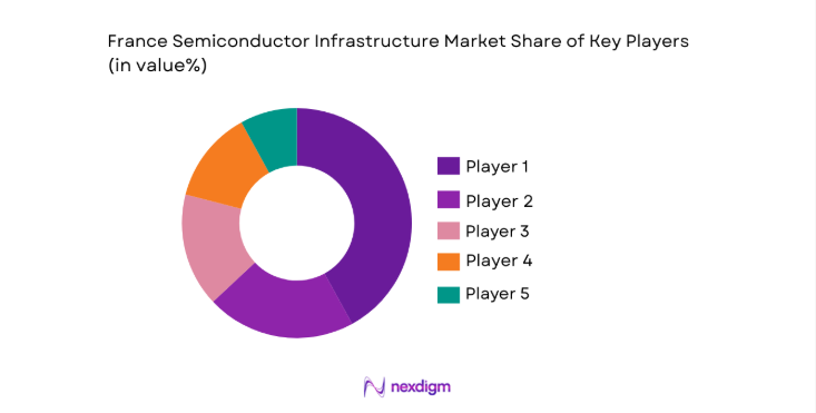
France Semiconductor Infrastructure market is moderately consolidated, characterized by strong presence of global semiconductor equipment manufacturers, engineering procurement construction specialists, industrial gas suppliers, and domestic semiconductor manufacturers with integrated infrastructure capabilities. Major players influence technology standards, fab construction models, and supply ecosystems through strategic partnerships with European semiconductor programs and long-term fabrication expansion contracts.
| Company Name | Establishment Year | Headquarters | Technology Focus | Market Reach | Key Products | Revenue | Fab Infrastructure Integration Capability |
| ASML Holding | 1984 | Netherlands | ~ | ~ | ~ | ~ | ~ |
| Applied Materials | 1967 | USA | ~ | ~ | ~ | ~ | ~ |
| Lam Research | 1980 | USA | ~ | ~ | ~ | ~ | ~ |
| STMicroelectronics | 1987 | Switzerland/France | ~ | ~ | ~ | ~ | ~ |
| Air Liquide Electronics | 1902 | France | ~ | ~ | ~ | ~ | ~ |
France Semiconductor Infrastructure Market Analysis
Growth Drivers
European semiconductor sovereignty funding and fab expansion programs
France semiconductor infrastructure expansion is strongly driven by coordinated European and national investment initiatives designed to localize semiconductor manufacturing capacity and reduce dependence on external supply chains. Public funding frameworks under the European Chips Act and national industrial programs have enabled large-scale fabrication and infrastructure projects, including subsidies for advanced wafer fabrication plants and compound semiconductor facilities. Government-backed investments in fabrication capacity, cleanroom construction, and utilities systems are directly increasing infrastructure demand across the semiconductor ecosystem. Strategic projects such as the multi-billion-euro Crolles 300 mm fab expansion supported by substantial state subsidies illustrate how policy-led capital deployment accelerates facility construction and equipment installation. Public incentives also lower financial risk for private semiconductor firms, encouraging joint ventures, research pilot lines, and advanced packaging infrastructure development in France. Infrastructure demand is further reinforced by funding allocated to semiconductor materials and substrate manufacturing expansion, including silicon-on-insulator and compound wafer production facilities. These programs collectively stimulate procurement of lithography, deposition, etch, and metrology infrastructure as fabrication capacity scales. Industrial policy alignment with European strategic autonomy goals ensures sustained multiyear infrastructure pipelines rather than cyclical investment patterns. National semiconductor strategies also emphasize domestic ecosystem clustering, which increases demand for integrated semiconductor campuses and utilities infrastructure. The result is a structurally supported infrastructure growth cycle anchored in sovereign semiconductor manufacturing ambitions across France and Europe.
Automotive electrification and power semiconductor manufacturing localization
France semiconductor infrastructure demand is accelerating due to structural growth in electric vehicle and industrial power electronics markets requiring localized semiconductor production capacity. Automotive applications represent one of the largest semiconductor demand sources in France, particularly for power devices and automotive microcontrollers, driving investment in dedicated fabrication and packaging infrastructure. Electrification trends across European automotive manufacturing hubs are increasing requirements for silicon carbide and power semiconductor production lines, which necessitate specialized wafer fabrication equipment, cleanroom environments, and high-precision process infrastructure. Domestic automotive semiconductor demand encourages integrated device manufacturers to expand local wafer fabrication capacity to ensure supply resilience for vehicle manufacturers and aerospace electronics producers. Infrastructure expansion also includes advanced packaging and testing facilities designed for automotive-grade semiconductor reliability standards. Localization of automotive semiconductor production reduces supply chain risks exposed during global chip shortages, further motivating investment in national fabrication infrastructure. France’s strong automotive and aerospace industrial base creates sustained long-term demand for power and mixed-signal semiconductor production infrastructure. Industrial electrification and renewable energy systems add additional demand for power semiconductor manufacturing facilities. These demand-side drivers translate directly into sustained fab construction, equipment procurement, and utilities infrastructure investment across the France semiconductor ecosystem.
Market Challenges
Extreme capital intensity and financing complexity of advanced semiconductor fabs
France semiconductor infrastructure development faces structural constraints due to exceptionally high capital requirements associated with advanced fabrication facilities and associated utilities infrastructure. Leading-edge semiconductor fabs require multi-billion-dollar investments covering cleanroom construction, lithography systems, process equipment, and specialized energy and water systems, creating financial barriers even for large semiconductor firms. Financing complexity is amplified by long payback periods and technology obsolescence risks, which increase reliance on public subsidies and joint-venture funding structures. European fab projects have experienced delays and scaling challenges due to funding gaps, cost overruns, and shifting corporate investment priorities, illustrating vulnerability of infrastructure expansion to financial constraints. Semiconductor infrastructure projects also face competition for capital from regions offering larger subsidies or lower construction costs, reducing investment attractiveness. Capital intensity further extends to supporting infrastructure such as industrial gases, chemical supply systems, and automation networks required for modern fabs. The need for continuous technology upgrades to remain competitive increases lifecycle infrastructure expenditure beyond initial construction costs. Economic downturns in semiconductor demand cycles can reduce corporate capital expenditure, delaying or scaling back infrastructure projects. These financial challenges collectively limit the pace and scale of semiconductor infrastructure expansion in France despite strong policy support.
Energy, water, and environmental permitting constraints in fabrication infrastructure deployment
Semiconductor fabrication infrastructure in France faces significant challenges related to resource intensity and environmental compliance requirements associated with modern fabs. Advanced semiconductor manufacturing facilities consume large volumes of electricity, ultrapure water, and specialty chemicals, creating infrastructure strain in regions with energy transition pressures and water management regulations. Environmental permitting processes for fab construction and utilities systems are lengthy and complex due to strict European environmental standards and local land-use regulations. Semiconductor fabs also require specialized waste treatment, emissions control, and chemical handling infrastructure, increasing regulatory scrutiny and project timelines. Energy cost volatility in Europe raises operational expenditure risks for semiconductor manufacturers, affecting investment decisions for infrastructure deployment. Resource constraints are particularly relevant in high-tech industrial clusters where multiple fabs compete for utilities capacity. Environmental approval delays have contributed to slower progress in European semiconductor fabrication projects compared with global competitors. Sustainability requirements also increase infrastructure costs through adoption of energy-efficient systems and water recycling technologies. These regulatory and resource constraints collectively slow infrastructure construction and increase total project cost and complexity in France semiconductor infrastructure development.
Opportunities
Expansion of compound semiconductor and silicon carbide fabrication infrastructure
France semiconductor infrastructure market presents strong opportunity through rapid growth in compound semiconductor and silicon carbide manufacturing required for electric vehicles, renewable energy systems, and industrial power electronics. Demand for wide-bandgap semiconductors is increasing across automotive electrification and high-efficiency power conversion applications, requiring specialized wafer fabrication and epitaxy infrastructure distinct from conventional silicon fabs. France hosts established compound semiconductor research and manufacturing capabilities, enabling expansion of dedicated silicon carbide and gallium nitride production facilities. Infrastructure development in this segment includes epitaxy reactors, advanced wafer processing tools, and specialized cleanroom environments designed for power semiconductor manufacturing. European automotive manufacturers’ shift toward electric drivetrains reinforces long-term demand for localized compound semiconductor production capacity. Public semiconductor programs prioritize power electronics as a strategic technology area, supporting infrastructure investment in this segment. Compound semiconductor fabs typically involve smaller but more specialized infrastructure projects, enabling faster deployment compared with leading-edge logic fabs. Growth in renewable energy and industrial electrification further increases demand for power semiconductor manufacturing infrastructure. This technology transition creates a sustained opportunity pipeline for specialized semiconductor infrastructure development in France.
Advanced packaging and heterogeneous integration facility development
France semiconductor infrastructure market offers major opportunity through expansion of advanced packaging and heterogeneous integration facilities supporting next-generation semiconductor architectures. Semiconductor performance improvements increasingly rely on advanced packaging technologies such as panel-level packaging, system-in-package, and chiplet integration, which require dedicated manufacturing infrastructure distinct from wafer fabrication. Investments in advanced packaging pilot lines and production facilities are already emerging in France, reflecting strategic shift toward value-added semiconductor manufacturing stages. Advanced packaging infrastructure includes high-precision assembly lines, bonding equipment, metrology systems, and contamination-controlled environments optimized for multi-die integration. Localization of packaging and testing capacity reduces dependence on Asian OSAT providers and strengthens European semiconductor supply chain resilience. Integration of heterogeneous semiconductor components for automotive, AI, and aerospace applications increases demand for advanced packaging infrastructure within France. Packaging facilities also complement domestic wafer fabrication by enabling full semiconductor value-chain integration. European semiconductor policy increasingly emphasizes packaging sovereignty alongside wafer manufacturing capacity. These structural technology shifts position advanced packaging infrastructure as a major growth opportunity within France semiconductor ecosystem development
Major Players
- ASML Holding
- Applied Materials
- Lam Research
- Tokyo Electron
- KLA Corporation
- ASM International
- Soitec
- Air Liquide Electronics
- Linde Engineering
- Exyte
- Technip Energies
- STMicroelectronics
- CEA-Leti
- Schneider Electric
- Merck Electronics
Key Target Audience
- Semiconductor manufacturers
- Automotive semiconductor producers
- Fab construction contractors
- Industrial automation suppliers
- Semiconductor equipment manufacturers
- Investments and venture capitalist firms
- Government and regulatory bodies
- Industrial gas and utilities providers
Research Methodology
Step 1: Identification of Key Variables
Key semiconductor infrastructure variables including fabrication capacity additions, cleanroom space expansion, equipment intensity, and national funding allocations were mapped across France. Technology node transitions, wafer size migration, and fab utility requirements were identified as primary demand determinants influencing infrastructure spending patterns.
Step 2: Market Analysis and Construction
Infrastructure spending across fabrication, packaging, and utilities systems was aggregated using company disclosures, government semiconductor programs, and European semiconductor investment databases. Capacity additions and facility construction timelines were translated into market value through infrastructure intensity ratios and equipment installation benchmarks.
Step 3: Hypothesis Validation and Expert Consultation
Industry experts from semiconductor manufacturing, fab engineering, and equipment supply chains validated infrastructure cost assumptions, facility configuration trends, and regional investment drivers. Cross-verification with European semiconductor associations and public funding agencies ensured consistency of market structure and segmentation assumptions.
Step 4: Research Synthesis and Final Output
Validated datasets and expert inputs were synthesized into segmentation, competitive positioning, and growth modeling frameworks specific to France semiconductor infrastructure. Market sizing, trend analysis, and strategic outlook were structured into a comprehensive research narrative aligned with semiconductor ecosystem dynamics and investment cycles.
- Executive Summary
- Research Methodology (Definitions, Scope, Industry Assumptions, Market Sizing Approach, Primary & Secondary Research Framework, Data Collection & Verification Protocol, Analytic Models & Forecast Methodology, Limitations & Research Validity Checks)
- Market Definition and Scope
- Value Chain & Stakeholder Ecosystem
- Regulatory / Certification Landscape
- Sector Dynamics Affecting Demand
- Strategic Initiatives & Infrastructure Growth

- Growth Drivers
European Chips Act driven fabrication investments
Automotive semiconductor localization initiatives
Expansion of advanced node manufacturing capacity
Public funding for strategic semiconductor autonomy
Growth of power and compound semiconductor fabs| - Market Challenges
High capital intensity of advanced fabs
Energy and water resource constraints
Supply chain dependency on non EU equipment
Skilled workforce shortages in fab engineering
Lengthy environmental and construction approvals - Market Opportunities
Expansion of compound semiconductor infrastructure
Public private partnerships for mega fabs
Modernization of legacy European fabs - Trends
Shift toward 300mm and advanced packaging lines
Integration of AI based process control systems
Adoption of sustainable fab utilities infrastructure
Growth in heterogeneous integration facilities
Localization of semiconductor supply chains - Government Regulations & Defense Policy
EU Chips Act subsidy and localization mandates
National security screening for semiconductor assets
Environmental compliance for high resource fabs - SWOT Analysis
- Stakeholder and Ecosystem Analysis
- Porter’s Five Forces Analysis
- Competition Intensity and Ecosystem Mapping
- By Market Value, 2020-2025
- By Installed Units, 2020-2025
- By Average System Price, 2020-2025
- By System Complexity Tier, 2020-2025
- By System Type (In Value%)
Wafer Fabrication Equipment Infrastructure
Semiconductor Assembly and Packaging Lines
Cleanroom and Contamination Control Systems
Process Control and Metrology Infrastructure
Utilities and Fab Support Systems - By Platform Type (In Value%)
300mm Wafer Fabrication Facilities
200mm Wafer Fabrication Facilities
Advanced Packaging Facilities
R&D Pilot Lines
Integrated Semiconductor Manufacturing Campuses - By Fitment Type (In Value%)
Greenfield Fab Installations
Brownfield Fab Expansions
Modular Fab Units
Retrofit and Modernization Projects
Turnkey Fab Infrastructure - By End User Segment (In Value%)
Integrated Device Manufacturers
Foundries and Contract Manufacturers
Outsourced Semiconductor Assembly and Test Providers
Research Institutes and Semiconductor Labs
Automotive Semiconductor Producers - By Procurement Channel (In Value%)
Direct OEM Procurement
Engineering Procurement Construction Contracts
Government Supported Consortia Procurement
Strategic Technology Partnerships
Distributor and Integrator Channels
- Market structure and competitive positioning
Market share snapshot of major players - Cross Comparison Parameters (Technology Node Capability, Wafer Size Support, Fab Scale, Automation Level, Energy Efficiency, Localization Strategy, Packaging Capability, EPC Integration, R&D Collaboration)
- SWOT Analysis of Key Competitors
- Pricing & Procurement Analysis
- Key Players
ASML Holding
Applied Materials
Lam Research
Tokyo Electron
KLA Corporation
ASM International
Soitec
Air Liquide Electronics
Linde Engineering
Exyte
Technip Energies
STMicroelectronics Infrastructure Division
CEA Leti Fab Services
Schneider Electric Industrial Automation
Merck Electronics
- IDMs expanding domestic fabrication resilience
- Automotive chipmakers investing in power semiconductors
- Research labs scaling pilot fabrication capabilities
- OSAT firms localizing advanced packaging capacity
- Forecast Market Value, 2026-2035
- Forecast Installed Units, 2026-2035
- Price Forecast by System Tier, 2026-2035
- Future Demand by Platform, 2026-2035


 Request a Sample
 Ask for Customization
 Get a Quote
 Enquire Now