
 Download PDF
 Download PDF
Market Overview
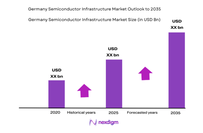
Germany semiconductor infrastructure market reached approximately USD ~ billion based on a recent historical assessment, supported by capital expenditure across wafer fabrication, power semiconductor expansion, and advanced packaging investments reported by European semiconductor industry associations and German federal economic data. Demand has been driven by automotive electrification chip requirements, EU semiconductor localization funding, and large-scale fab construction projects announced by major manufacturers, which accelerated infrastructure spending across cleanrooms, lithography systems, and utility supply platforms nationwide.
Dresden, Magdeburg, and Munich have emerged as dominant semiconductor infrastructure hubs due to dense supplier ecosystems, established research institutes, and proximity to automotive and industrial electronics clusters. Saxony’s “Silicon Saxony” network concentrates fabrication facilities, equipment vendors, and engineering talent, while Bavaria hosts power semiconductor leaders and photonics suppliers. Magdeburg’s prominence is linked to new mega-fab developments and government-supported industrial zones, reinforcing Germany’s regional specialization in advanced semiconductor manufacturing infrastructure.
Market Segmentation
By Product Type
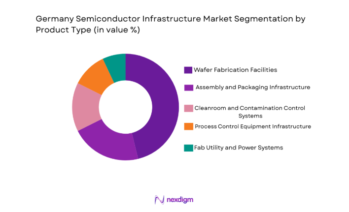
Germany Semiconductor Infrastructure Market market is segmented by product type into Wafer Fabrication Facilities, Assembly and Packaging Infrastructure, Cleanroom Systems, Process Control Equipment Infrastructure, and Fab Utility and Power Systems. Recently, Wafer Fabrication Facilities has a dominant market share due to factors such as large-scale fab construction programs, EU-backed semiconductor sovereignty initiatives, and rising automotive chip production localization. Germany’s strong integrated device manufacturer base and new mega-fab announcements have significantly elevated capital allocation toward fabrication infrastructure compared with downstream packaging or utilities segments.
By Platform Type
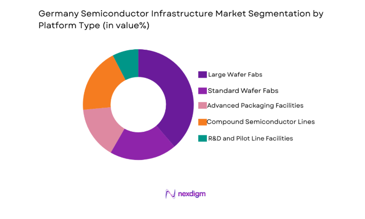
Germany Semiconductor Infrastructure Market market is segmented by platform type into large Wafer Fabs, standard Wafer Fabs, Advanced Packaging Facilities, Compound Semiconductor Lines, and R&D Pilot Lines. Recently, 300mm Wafer Fabs has a dominant market share due to factors such as advanced node production requirements, automotive power semiconductor scaling, and efficiency advantages in high-volume manufacturing. Germany’s strategic investments and multinational fab expansions are concentrated on 300mm platforms, which require significantly higher infrastructure spending across lithography, automation, and cleanroom engineering compared with legacy or pilot fabrication environments.
Competitive Landscape
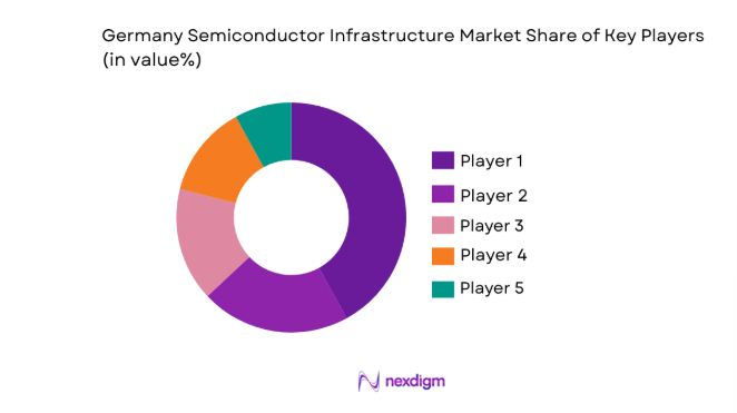
Germany semiconductor infrastructure market exhibits moderate consolidation with a mix of global equipment suppliers, engineering contractors, and domestic semiconductor manufacturers shaping infrastructure deployment. Major players influence technology standards, project scale, and supply chain localization through long-term fab investments and partnerships with German industrial clusters. The competitive environment is characterized by vertically integrated semiconductor firms and specialized engineering providers supporting advanced fabrication expansion across regional hubs.
| Company Name | Establishment Year | Headquarters | Technology Focus | Market Reach | Key Products | Revenue | Fab Infrastructure Capability |
| Infineon Technologies | 1999 | Neubiberg, Germany | ~ | ~ | ~ | ~ | ~ |
| GlobalFoundries Dresden | 2009 | Dresden, Germany | ~ | ~ | ~ | ~ | ~ |
| Bosch Semiconductor | 1886 | Stuttgart, Germany | ~ | ~ | ~ | ~ | ~ |
| Siltronic AG | 1968 | Munich, Germany | ~ | ~ | ~ | ~ | ~ |
| X-FAB Silicon Foundries | 1992 | Erfurt, Germany | ~ | ~ | ~ | ~ | ~ |
Germany Semiconductor Infrastructure Market Analysis
Growth Drivers
Automotive Electrification Semiconductor Demand Expansion
Germany’s leadership in automotive manufacturing has accelerated domestic semiconductor infrastructure investment as electric vehicle architectures require significantly higher chip content across power electronics, battery management, sensing, and control systems. Automakers and suppliers have pursued supply chain resilience strategies after recent chip shortages disrupted vehicle production, leading to long-term localization agreements with semiconductor manufacturers and infrastructure providers. Power semiconductor technologies such as silicon carbide and gallium nitride are increasingly produced in Germany due to proximity to automotive engineering centers and reliability certification ecosystems. Government industrial policy has reinforced this shift through subsidies and incentives for semiconductor fabs supporting automotive and industrial applications. The transition toward autonomous driving and advanced driver assistance systems has further increased demand for high-performance logic and sensor chips requiring advanced fabrication capacity. Infrastructure spending has therefore expanded across wafer fabs, cleanrooms, and lithography installations dedicated to automotive semiconductor production. Germany’s Tier-1 suppliers have also entered semiconductor partnerships, amplifying infrastructure requirements for packaging and testing facilities. As vehicle electrification scales across Europe, sustained semiconductor infrastructure expansion in Germany is expected to remain structurally linked to automotive sector transformation.
European Semiconductor Sovereignty and Public Funding Programs
European strategic policy initiatives aimed at reducing dependence on external semiconductor supply chains have significantly stimulated infrastructure investment within Germany as a core manufacturing hub. Funding frameworks under regional semiconductor acts have enabled large-scale fab construction projects and technology upgrades that would otherwise face capital intensity barriers. Germany’s established engineering base and industrial ecosystem position it as a primary beneficiary of European semiconductor localization strategies, attracting multinational manufacturers seeking subsidized expansion. Public funding has been directed not only toward fabrication facilities but also toward cleanroom engineering, materials supply, and advanced packaging infrastructure. Cross-border collaboration programs have strengthened research and pilot line facilities, enhancing Germany’s role in next-generation semiconductor technology development. Infrastructure investment has expanded into compound semiconductor and advanced node capabilities aligned with European industrial priorities. Regional governments have supported industrial parks, utilities infrastructure, and workforce training programs essential for semiconductor fabs. These coordinated policy and funding mechanisms have structurally increased infrastructure spending across Germany’s semiconductor value chain.
Market Challenges
High Capital Intensity and Long Payback Cycles of Semiconductor Fabs
Semiconductor infrastructure projects in Germany require exceptionally high upfront capital expenditures due to advanced fabrication technology, stringent cleanroom standards, and complex utility systems, creating financial barriers for both domestic and international investors. Construction of a modern 300mm wafer fabrication facility involves billions of dollars in equipment, materials, and engineering services, with long development timelines before production ramp-up and revenue generation. Investors face extended payback cycles influenced by technology obsolescence risk, cyclical semiconductor demand, and rapid node evolution requiring continuous reinvestment. Germany’s regulatory environment adds additional cost layers through environmental compliance, permitting processes, and energy efficiency standards that increase project complexity. Smaller semiconductor firms often lack financial capacity to undertake infrastructure expansion without external funding or partnerships. Cost escalation risks during construction, including materials inflation and equipment lead times, further challenge project viability. Infrastructure projects also require specialized talent and supply chains that may constrain timelines and budgets. These financial and operational barriers collectively slow semiconductor infrastructure expansion despite strong demand drivers.
Energy Costs and Industrial Infrastructure Constraints
Semiconductor manufacturing infrastructure in Germany faces significant operational cost pressures due to high industrial electricity prices and energy transition policies affecting energy-intensive fabrication processes. Wafer fabrication facilities require continuous power supply, temperature control, and ultrapure water systems, making energy costs a major component of operating expenditure compared with competing semiconductor regions. Germany’s industrial energy pricing and grid transition dynamics can reduce global cost competitiveness for semiconductor manufacturers considering infrastructure investments. Infrastructure projects must also integrate renewable energy and sustainability requirements that increase capital and engineering complexity. Utility infrastructure availability, including water supply and waste management, can constrain fab site selection and expansion capacity in certain regions. Energy supply reliability and long-term price stability are critical for semiconductor fabs operating continuously with minimal downtime tolerance. Manufacturers therefore face strategic trade-offs between Germany’s ecosystem advantages and operational cost structures. These constraints influence investment decisions and may shift certain semiconductor infrastructure expansion toward lower-cost regions.
Opportunities
Expansion of Power Semiconductor and Compound Semiconductor Manufacturing
Germany’s strong automotive and industrial base creates substantial opportunity for semiconductor infrastructure dedicated to power electronics and compound semiconductor technologies such as silicon carbide and gallium nitride. Electrification of vehicles, renewable energy systems, and industrial automation drives demand for high-efficiency power devices that Germany already leads in design and application engineering. Infrastructure investment in specialized fabrication lines for wide-bandgap semiconductors is increasing due to their performance advantages in high-voltage and high-temperature applications. Germany’s existing semiconductor manufacturers and research institutes provide a foundation for scaling compound semiconductor production capacity. Government incentives and European industrial strategies further support expansion in these strategic technologies. Supply chain localization goals encourage domestic production of power semiconductors used in energy and mobility sectors. Infrastructure providers specializing in materials, epitaxy, and packaging benefit from this shift toward compound semiconductor manufacturing. The convergence of electrification trends and technological specialization positions Germany as a global hub for power semiconductor infrastructure growth.
Advanced Packaging and Heterogeneous Integration Infrastructure Development
Semiconductor innovation is increasingly driven by advanced packaging technologies such as chiplet architectures, 3D integration, and heterogeneous system assembly, creating infrastructure opportunities beyond traditional wafer fabrication in Germany. European semiconductor strategies emphasize strengthening advanced packaging capabilities to complement fabrication capacity and reduce reliance on external assembly ecosystems. Germany’s strong precision engineering and equipment manufacturing base supports development of advanced packaging infrastructure including bonding, interconnect, and testing systems. Automotive and industrial semiconductor applications require highly reliable packaging solutions, encouraging domestic infrastructure investment in these technologies. Collaboration between semiconductor firms, research institutes, and equipment suppliers accelerates packaging innovation and pilot line deployment. Advanced packaging infrastructure also enables integration of compound semiconductors and sensors with logic chips, supporting emerging electronic architectures. Public funding programs increasingly target packaging capabilities as a strategic gap in European semiconductor value chains. These factors create sustained opportunity for Germany to expand semiconductor infrastructure into advanced packaging domains.
Future Outlook
Germany semiconductor infrastructure market is expected to expand steadily over the next five years supported by continued European semiconductor localization policies, automotive electrification demand, and large-scale fab construction programs. Technological progress in power semiconductors, advanced nodes, and packaging will drive new infrastructure investments across fabrication and assembly. Regulatory support through funding and industrial policy will sustain capital flows into semiconductor ecosystems. Demand growth from mobility, energy, and industrial digitalization sectors will reinforce Germany’s position as Europe’s primary semiconductor manufacturing hub.
Major Players
- Infineon Technologies
- GlobalFoundries Dresden
- Bosch Semiconductor
- Siltronic AG
- X-FAB Silicon Foundries
- ZEISS SMT
- ASML Berlin
- ExyteGmbH
- Linde Engineering
- SUSSMicroTec
- AixtronSE
- Pfeiffer Vacuum Technology
- Edwards Vacuum
- Trumpf Photonic Systems
- Applied Materials Germany
Key Target Audience
- Semiconductor manufacturers
- Automotive electronics companies
- Industrial electronics firms
- Fab construction contractors
- Semiconductor equipment suppliers
- Government and regulatory bodies
- Investment and venture capitalist firms
- Materials and chemicals suppliers
Research Methodology
Step 1: Identification of Key Variables
Key semiconductor infrastructure variables including fabrication capacity, equipment investment, cleanroom scale, and regional policy incentives were identified through industry databases, government reports, and semiconductor association publications. Supply chain actors across equipment, materials, and manufacturing segments were mapped to define infrastructure scope.
Step 2: Market Analysis and Construction
Market size and segmentation were constructed using capital expenditure data, fab project announcements, and equipment deployment statistics across Germany’s semiconductor hubs. Infrastructure components were categorized by product and platform to quantify market distribution and dominant segments.
Step 3: Hypothesis Validation and Expert Consultation
Preliminary findings were validated through expert interviews with semiconductor engineers, fab planners, and industry analysts to confirm infrastructure trends, investment drivers, and technology shifts. Regional policy and funding impacts were cross-checked against official industrial strategy documents.
Step 4: Research Synthesis and Final Output
Validated data and qualitative insights were synthesized into structured market analysis covering segmentation, competition, and growth dynamics. Final outputs were reviewed for consistency with semiconductor infrastructure definitions and Germany’s industrial context before report preparation.
- Executive Summary
- Research Methodology (Definitions, Scope, Industry Assumptions, Market Sizing Approach, Primary & Secondary Research Framework, Data Collection & Verification Protocol, Analytic Models & Forecast Methodology, Limitations & Research Validity Checks)
- Market Definition and Scope
- Value Chain & Stakeholder Ecosystem
- Regulatory / Certification Landscape
- Sector Dynamics Affecting Demand
- Strategic Initiatives & Infrastructure Growth

- Growth Driver
Expansion of European semiconductor sovereignty programs
Rising automotive chip production localization
Investment incentives under regional semiconductor acts
Shift toward advanced node fabrication capabilities
Growth in power semiconductor manufacturing demand - Market Challenges
High capital intensity of advanced fabs
Energy cost volatility in industrial regions
Skilled semiconductor workforce shortages
Long equipment lead times and supply bottlenecks
Regulatory complexity in environmental compliance - Market Opportunities
Development of automotive and power semiconductor hubs
Public private partnerships for fab construction
Expansion of compound semiconductor capacity - Trends
Adoption of EUV enabled fabrication facilities
Integration of AI driven fab automation systems
Growth of advanced packaging infrastructure
Localization of semiconductor supply chains
Sustainable and low energy fab designs - Government Regulations & Defense Policy
European Chips Act funding frameworks
Industrial energy transition mandates
Strategic semiconductor security initiatives - SWOT Analysis
- Stakeholder and Ecosystem Analysis
- Porter’s Five Forces Analysis
- Competition Intensity and Ecosystem Mapping
- By Market Value, 2020-2025
- By Installed Units, 2020-2025
- By Average System Price, 2020-2025
- By System Complexity Tier, 2020-2025
- By System Type (In Value%)
Wafer Fabrication Facilities
Semiconductor Assembly and Packaging Lines
Cleanroom and Contamination Control Systems
Process Control and Metrology Infrastructure
Power and Utility Supply Systems - By Platform Type (In Value%)
Large Wafer Fabs
Standard Wafer Fabs
Advanced Packaging Facilities
R&D and Pilot Fabrication Lines
Compound Semiconductor Production Lines - By Fitment Type (In Value%)
Greenfield Fab Installations
Brownfield Fab Expansions
Modular Fab Units
Retrofitted Legacy Facilities
Collaborative Research Facilities - By End User Segment (In Value%)
Integrated Device Manufacturers
Pure Play Foundries
Automotive Semiconductor Producers
Industrial Electronics Manufacturers
Research Institutes and Universities - By Procurement Channel (In Value%)
Direct OEM Procurement
EPC and Turnkey Contractors
Government Supported Consortia
Strategic Technology Partnerships
Equipment Leasing and Financing Models
- Market structure and competitive positioning
Market share snapshot of major players - Cross Comparison Parameters (Technology Node Capability, Fab Construction Expertise, Cleanroom Engineering, Automation Integration, EUV Infrastructure Readiness, Packaging Capability, Project Scale, Energy Efficiency Design, Local Partnership Strength)
- SWOT Analysis of Key Competitors
- Pricing & Procurement Analysis
- Key Players
ASML Berlin
ZEISS SMT
Infineon Technologies
GlobalFoundries Dresden
Siltronic AG
Bosch Semiconductor
X-FAB Silicon Foundries
Pfeiffer Vacuum Technology
SUSS MicroTec
Aixtron SE
Linde Engineering
Exyte GmbH
Trumpf Photonic Systems
Edwards Vacuum
Applied Materials Germany
- Automotive semiconductor producers prioritizing local fab access
- Integrated device manufacturers expanding EU production bases
- Research institutes driving pilot line infrastructure demand
- Industrial electronics firms seeking supply chain resilience
- Forecast Market Value, 2026-2035
- Forecast Installed Units, 2026-2035
- Price Forecast by System Tier, 2026-2035
- Future Demand by Platform, 2026-2035


 Request a Sample
 Ask for Customization
 Get a Quote
 Enquire Now