
 Download PDF
 Download PDF
Market Overview
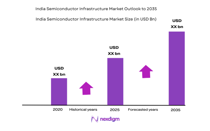
India semiconductor infrastructure market reached approximately USD ~ billion based on a recent historical assessment, reflecting cumulative investments in wafer fabrication facilities, ATMP plants, and cleanroom infrastructure under national semiconductor missions and private consortium projects. The market is driven by large-scale fab announcements, government capital subsidies, and rising domestic electronics production value exceeding USD ~ billion, which is creating sustained demand for ultra-pure utilities, advanced cleanrooms, and semiconductor-grade industrial infrastructure across fabrication and packaging ecosystems.
Gujarat and Karnataka dominate India semiconductor infrastructure deployment due to proactive state semiconductor policies, land allocation for fab clusters, and established electronics manufacturing ecosystems anchored by Ahmedabad-Dholera and Bengaluru-Mysuru industrial corridors. These regions attract fabrication and packaging projects through reliable power and water infrastructure, proximity to ports and logistics hubs, and concentration of semiconductor design firms and engineering talent pools that enable integrated fab-to-design ecosystems within localized semiconductor manufacturing zones.
Market Segmentation
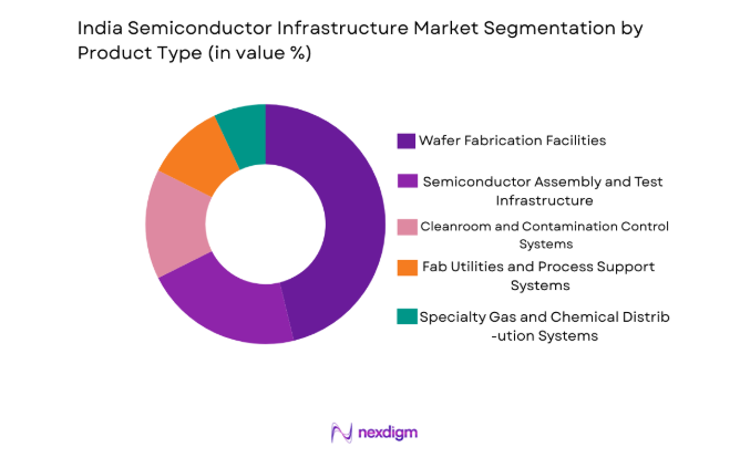
By Product Type
India semiconductor infrastructure market is segmented by product type into wafer fabrication facilities, semiconductor assembly and test infrastructure, cleanroom and contamination control systems, fab utilities and process support systems, and specialty gas and chemical distribution systems. Recently, wafer fabrication facilities has a dominant market share due to factors such as demand patterns, brand presence, infrastructure availability, or consumer preference.
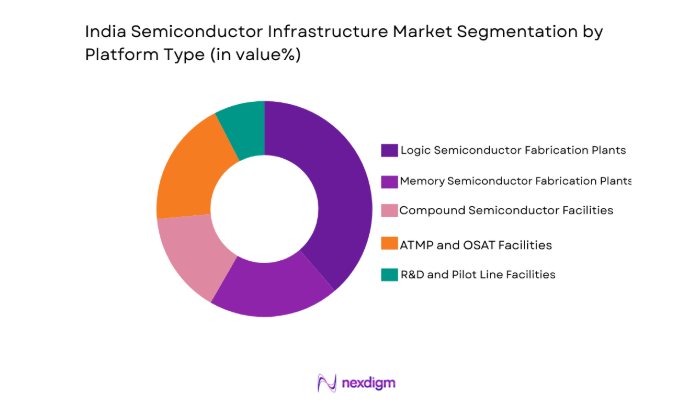
By Platform Type
India semiconductor infrastructure market is segmented by product type into logic semiconductor fabrication plants, memory semiconductor fabrication plants, compound semiconductor facilities, ATMP and OSAT facilities, and R&D and pilot line facilities. Recently, logic semiconductor fabrication plants has a dominant market share due to factors such as demand patterns, brand presence, infrastructure availability, or consumer preference.
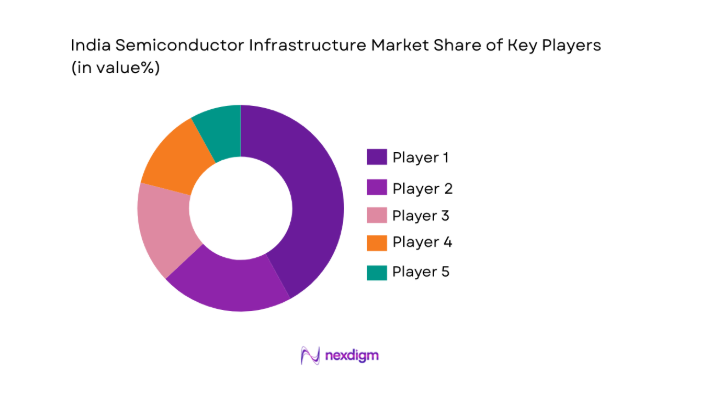
Competitive Landscape
India semiconductor infrastructure market shows a moderately concentrated competitive structure where a limited number of engineering conglomerates, semiconductor infrastructure specialists, and global equipment ecosystem firms influence project execution, technology standards, and supply chains. Large domestic industrial groups and international semiconductor infrastructure providers dominate through EPC capabilities, technology partnerships, and integrated fab development expertise, while emerging local semiconductor ventures expand through government incentives and strategic alliances.
| Company Name | Establishment Year | Headquarters | Technology Focus | Market Reach | Key Products | Revenue | Semiconductor Infrastructure Capability |
| Tata Electronics | 2020 | India | ~ | ~ | ~ | ~ | ~ |
| Vedanta Semiconductors | 2021 | India | ~ | ~ | ~ | ~ | ~ |
| Larsen and Toubro | 1938 | India | ~ | ~ | ~ | ~ | ~ |
| Foxconn | 1974 | Taiwan | ~ | ~ | ~ | ~ | ~ |
| Tower Semiconductor | 1993 | Israel | ~ | ~ | ~ | ~ | ~ |
India Semiconductor Infrastructure Market Analysis
Growth Drivers
Government-Backed Semiconductor Mission and Capital Subsidy Programs
India’s semiconductor infrastructure market expansion is fundamentally shaped by unprecedented state-backed capital subsidy frameworks designed to catalyze domestic fabrication and packaging capacity creation at scale across strategic electronics sectors, where national semiconductor missions allocate tens of billions of dollars in fiscal incentives to offset the extreme upfront capital costs associated with wafer fabrication and advanced packaging infrastructure projects that typically exceed several billion dollars per facility, thereby directly improving project bankability for private investors and global semiconductor firms considering geographic diversification of fabrication footprints. These policy frameworks encompass capital expenditure subsidies, production-linked incentives, infrastructure support, and long-term procurement commitments that collectively reduce financial risk for fab developers and enable accelerated project approvals and land allocation within designated semiconductor manufacturing clusters. As semiconductor manufacturing requires highly specialized ultra-pure utilities, vibration-controlled structures, and contamination-free cleanroom environments, subsidy-enabled fab construction automatically triggers large downstream demand for semiconductor-grade industrial infrastructure including cleanroom systems, high-purity gas and chemical distribution networks, process utilities, and automated material handling facilities. Government programs also mandate local value addition and domestic ecosystem development, encouraging localization of semiconductor infrastructure supply chains and engineering services that further expand domestic infrastructure spending across construction, utilities, and process integration domains. Public investment additionally finances semiconductor research fabs, pilot lines, and packaging facilities in collaboration with industry partners, expanding the infrastructure market beyond commercial wafer fabs into R&D and strategic electronics manufacturing segments. State governments complement national incentives through land grants, tax exemptions, and infrastructure provisioning for semiconductor parks, enabling cluster-based fab infrastructure development that aggregates multiple facilities and amplifies total infrastructure demand. These coordinated fiscal and industrial policies effectively transform semiconductor infrastructure from isolated industrial investments into national strategic programs with long-term funding visibility, ensuring sustained pipeline visibility for infrastructure providers and engineering firms. The policy-driven project pipeline also attracts global semiconductor ecosystem suppliers including cleanroom specialists, fab utility providers, and process infrastructure firms to establish local operations, thereby deepening domestic infrastructure capacity and reinforcing market growth momentum. Consequently, subsidy-enabled semiconductor manufacturing programs remain the single largest structural driver of India semiconductor infrastructure market expansion by directly unlocking capital-intensive fab and packaging infrastructure deployment across multiple technology nodes and semiconductor segments.
Rapid Expansion of Domestic Electronics Manufacturing and Localization Demand
India’s accelerating electronics manufacturing sector creates structural downstream demand for semiconductor fabrication and packaging infrastructure as domestic production of smartphones, automotive electronics, industrial electronics, and consumer devices expands to serve both domestic consumption and export markets under localization initiatives that prioritize indigenous component supply chains and reduced import dependence for critical semiconductor components. As electronics production value scales into hundreds of billions of dollars annually, supply chain resilience considerations motivate device manufacturers and system integrators to secure local semiconductor sourcing through domestic fabs and assembly facilities, thereby generating sustained demand for semiconductor infrastructure investments across wafer fabrication, ATMP, and specialty semiconductor manufacturing domains. The localization push is particularly strong in automotive and power electronics segments where electrification, renewable energy systems, and industrial automation require power semiconductors and analog devices that are increasingly targeted for domestic production to ensure supply security and reduce exposure to global semiconductor shortages. Electronics manufacturing clusters concentrated in states such as Tamil Nadu, Karnataka, and Uttar Pradesh further amplify regional demand for semiconductor infrastructure as component suppliers seek proximity to assembly plants and original equipment manufacturers to optimize logistics, lead times, and supply chain integration. The scale of electronics demand also justifies development of semiconductor packaging and testing infrastructure, which typically precedes full wafer fabrication investments and creates intermediate infrastructure markets involving cleanrooms, utilities, and process integration systems. Government procurement programs for strategic electronics including defense and telecommunications equipment additionally reinforce localization requirements for semiconductor components, indirectly stimulating infrastructure investments in trusted semiconductor manufacturing facilities. Export-oriented electronics production targeting global markets further requires compliance with international semiconductor supply chain standards, motivating domestic firms to invest in advanced fabrication and packaging infrastructure aligned with global technology nodes and quality requirements. As domestic electronics manufacturing capacity continues expanding across multiple sectors, the associated semiconductor demand creates a structural pull for upstream fabrication and packaging infrastructure deployment within national borders. This demand-driven industrial expansion complements policy incentives and ensures that semiconductor infrastructure investments are anchored in real manufacturing consumption rather than purely strategic ambitions, thereby strengthening long-term market sustainability.
Market Challenges
Extreme Capital Intensity and Long Gestation Periods of Semiconductor Fabs
semiconductor fabrication facilities represent among the most capital-intensive industrial infrastructure projects globally, often requiring investments exceeding several billion dollars with construction timelines extending multiple years before revenue generation begins, creating substantial financial exposure and project execution risk for developers, lenders, and governments attempting to establish domestic semiconductor manufacturing capacity within emerging ecosystems that lack prior fab infrastructure experience. The magnitude of capital commitment required for cleanroom construction, ultra-pure utility systems, process equipment integration, and advanced facility engineering creates barriers to entry for domestic firms and necessitates complex financing structures involving public subsidies, consortium investments, and long-term supply agreements to secure economic viability. Extended gestation periods amplify risks associated with semiconductor market cyclicality, where global demand fluctuations or technology transitions during construction phases can affect projected utilization and profitability of new fabs before operations commence. Infrastructure developers must also coordinate with semiconductor equipment suppliers, technology licensors, and process partners whose availability and delivery schedules significantly influence project timelines, increasing execution complexity compared with conventional industrial infrastructure. Cost overruns and delays in specialized construction activities such as vibration-isolated foundations, contamination-controlled materials installation, and ultra-pure water and gas systems integration can escalate project budgets and erode financial returns, particularly in regions without established semiconductor construction supply chains. The need for highly specialized engineering expertise in semiconductor facility design and commissioning further constrains project scalability and increases dependence on foreign contractors and consultants, raising costs and limiting domestic capability development. Financing institutions may perceive semiconductor fab infrastructure as high-risk due to technological obsolescence risks and long payback periods, resulting in higher cost of capital or limited funding availability for projects lacking strong government backing. Operational ramp-up challenges after construction, including yield optimization and process stabilization, can delay revenue realization and extend return horizons, indirectly affecting infrastructure investment attractiveness. These structural financial and execution challenges collectively slow the pace of semiconductor infrastructure deployment despite strong policy intent and demand drivers, representing a fundamental constraint on market expansion.
Limited Domestic Ecosystem for Semiconductor-Grade Materials and Utilities
semiconductor manufacturing infrastructure depends critically on ultra-high-purity materials, specialty gases, precision chemicals, and contamination-free utility systems that require specialized supply chains and production capabilities rarely present in emerging semiconductor ecosystems, creating dependence on imported materials and foreign suppliers that increases project complexity, costs, and operational vulnerability for domestic semiconductor infrastructure development. High-purity gases, specialty chemicals, and advanced cleanroom materials must meet stringent semiconductor-grade standards, and absence of local suppliers necessitates import logistics, storage infrastructure, and quality assurance systems that complicate facility design and increase capital expenditure. Utility infrastructure for semiconductor fabs including ultra-pure water generation, waste treatment, and stable power systems demands advanced engineering expertise and reliable upstream inputs, which may be constrained by regional infrastructure limitations such as water scarcity, grid instability, or environmental compliance requirements. Lack of domestic manufacturers for semiconductor facility components such as high-purity piping, valves, filtration systems, and contamination-controlled construction materials forces reliance on imported equipment with longer procurement lead times and foreign exchange exposure, affecting project timelines and costs. Limited domestic technical workforce trained in semiconductor facility operations and maintenance further complicates commissioning and sustained operation of infrastructure systems that require stringent contamination control and reliability standards. Environmental and safety regulations governing semiconductor chemicals and waste streams also require specialized infrastructure and compliance capabilities that domestic ecosystems are still developing, adding regulatory complexity to infrastructure deployment. Dependence on foreign ecosystem suppliers can expose semiconductor infrastructure projects to geopolitical trade restrictions, export controls, or supply disruptions affecting availability of critical materials and technologies. Localization of semiconductor infrastructure supply chains requires long-term investment and technology transfer partnerships that may not align with immediate project timelines, creating transitional challenges for early fab developments. These ecosystem gaps collectively constrain domestic semiconductor infrastructure scalability and increase reliance on international suppliers, representing a structural challenge for market maturation.
Opportunities
Development of Integrated Semiconductor Clusters and Fab Parks
India’s semiconductor infrastructure market presents significant opportunity through establishment of integrated semiconductor clusters that co-locate wafer fabrication plants, assembly and testing facilities, materials suppliers, equipment vendors, and research institutions within designated industrial zones, enabling shared utilities, logistics, and support infrastructure that reduces individual project costs while enhancing ecosystem efficiency and supply chain integration across semiconductor manufacturing value chains. Cluster-based fab parks allow centralized deployment of ultra-pure water plants, specialty gas networks, waste treatment facilities, and power infrastructure that can serve multiple semiconductor facilities simultaneously, improving capital efficiency and enabling scalable expansion of semiconductor infrastructure capacity within planned industrial corridors. Co-location of ecosystem participants within clusters also shortens supply chains for semiconductor materials and services, reducing logistics complexity and supporting just-in-time delivery requirements essential for semiconductor manufacturing operations. Semiconductor clusters attract specialized service providers including cleanroom maintenance firms, facility management specialists, and process integration consultants, deepening domestic infrastructure expertise and supporting sustained operational performance of semiconductor facilities. Government planning of semiconductor parks with pre-approved environmental clearances, land preparation, and infrastructure provisioning accelerates project timelines and reduces administrative barriers for investors, enhancing attractiveness of cluster-based semiconductor infrastructure development. Integrated clusters also support workforce development through proximity to training centers and research institutions, enabling talent pipelines aligned with semiconductor facility engineering and operations requirements. Cluster ecosystems encourage collaboration among semiconductor firms, research organizations, and suppliers that fosters innovation in facility design, process optimization, and infrastructure technologies tailored to domestic conditions. Export-oriented semiconductor clusters located near ports and logistics hubs improve global supply chain connectivity and support international semiconductor trade integration. As multiple semiconductor projects aggregate within clusters, cumulative infrastructure demand increases significantly, creating sustained opportunities for engineering firms, utility providers, and infrastructure developers. Integrated semiconductor clusters therefore represent a transformative opportunity to scale domestic semiconductor infrastructure efficiently while building long-term ecosystem competitiveness.
Localization of Semiconductor Materials and Infrastructure Supply Chains
expanding domestic production of semiconductor-grade materials, facility components, and utility systems offers substantial opportunity to reduce import dependence, lower infrastructure costs, and strengthen national semiconductor ecosystem resilience by fostering local manufacturing capabilities across high-purity chemicals, specialty gases, cleanroom materials, precision piping, and facility automation systems required for semiconductor fabrication and packaging infrastructure. Domestic production of semiconductor facility materials shortens procurement cycles, reduces foreign exchange exposure, and enables customization of infrastructure components for local environmental and operational conditions, improving project economics and scalability for semiconductor infrastructure developers. Localization initiatives also create new industrial sectors adjacent to semiconductor manufacturing, generating employment, technology transfer, and investment across advanced materials and industrial equipment domains. Partnerships between global semiconductor ecosystem suppliers and domestic firms can facilitate technology transfer and capability development in semiconductor-grade infrastructure materials and components, accelerating maturation of local supply chains while maintaining global quality standards. Government incentives for semiconductor ecosystem localization further support establishment of domestic production facilities for high-purity gases, chemicals, and cleanroom systems, directly expanding infrastructure market scope beyond construction into materials manufacturing segments. As domestic semiconductor manufacturing capacity grows, scale economies in localized materials production improve cost competitiveness relative to imports, reinforcing adoption of domestic infrastructure components in future fab and packaging projects. Local suppliers can also provide faster maintenance, replacement, and technical support services for semiconductor infrastructure systems, improving operational reliability and reducing downtime risks for fabs. Export potential for semiconductor infrastructure materials and components may emerge as domestic capabilities mature, positioning India as a regional supplier within global semiconductor ecosystems. Localization of semiconductor infrastructure supply chains thus represents a strategic opportunity to expand market depth, reduce costs, and enhance long-term competitiveness of domestic semiconductor manufacturing infrastructure.
Future Outlook
India semiconductor infrastructure market is expected to expand significantly over the next five years as multiple wafer fabrication and packaging projects transition from planning to construction phases under national semiconductor programs. Increasing localization of semiconductor materials, expansion of electronics manufacturing demand, and development of semiconductor clusters will accelerate infrastructure deployment across fabrication and ATMP facilities. Technological adoption of modular fabs, sustainable utilities, and automation-integrated facilities will reshape infrastructure design standards. Continued policy support and global semiconductor diversification strategies will sustain long-term infrastructure investment momentum.
Major Players
- Tata Electronics
- Vedanta Semiconductors
- Larsen and Toubro
- Foxconn
- Tower Semiconductor
- ISMC Analog Fab
- Adani Semiconductor Technologies
- SPEL Semiconductor
- Sahasra Semiconductors
- ASM Technologies
- Applied Materials
- Tokyo Electron
- Merck Electronics
- Technoprobe
- HCL Technologies
Key Target Audience
- Semiconductor manufacturers
- Electronics OEMs
- Automotive electronics firms
- Industrial electronics companies
- Investments and venture capitalist firms
- Government and regulatory bodies
- Specialty chemicals producers
- Industrial infrastructure developers
Research Methodology
Step 1: Identification of Key Variables
Key semiconductor infrastructure components, facility types, investment flows, and policy incentives were identified through secondary industry databases, government semiconductor mission documents, and corporate announcements. Variables included fab capacity, cleanroom scale, utilities infrastructure, and capital expenditure patterns across semiconductor projects.
Step 2: Market Analysis and Construction
Market sizing combined fab project investment tracking, semiconductor infrastructure cost benchmarks, and engineering EPC data to construct total infrastructure value across fabrication and packaging facilities. Segmentation analysis mapped system types and end-user demand across semiconductor manufacturing value chains.
Step 3: Hypothesis Validation and Expert Consultation
Findings were validated through consultations with semiconductor facility engineers, infrastructure EPC firms, and semiconductor ecosystem suppliers to confirm infrastructure cost structures, deployment timelines, and technology requirements across fabrication and ATMP projects.
Step 4: Research Synthesis and Final Output
Validated data and qualitative insights were synthesized into market structure, segmentation, and competitive analysis frameworks, ensuring consistency with semiconductor infrastructure investment pipelines and national semiconductor policy trajectories to produce final market assessment outputs.
- Executive Summary
- Research Methodology (Definitions, Scope, Industry Assumptions, Market Sizing Approach, Primary & Secondary Research Framework, Data Collection & Verification Protocol, Analytic Models & Forecast Methodology, Limitations & Research Validity Checks)
- Market Definition and Scope
- Value Chain & Stakeholder Ecosystem
- Regulatory / Certification Landscape
- Sector Dynamics Affecting Demand
- Strategic Initiatives & Infrastructure Growth

- Growth Drivers
Government semiconductor incentive schemes driving fab construction
Rising domestic electronics manufacturing and localization push
Strategic supply chain resilience initiatives in semiconductors
Global semiconductor firms diversifying fabrication geography
Growth in automotive and power electronics semiconductor demand - Market Challenges
High capital intensity and long payback periods for fabs
Limited domestic ecosystem for semiconductor grade materials
Infrastructure gaps in utilities reliability and purity standards
Dependence on foreign technology partners and equipment
Skilled workforce shortages in semiconductor engineering - Market Opportunities
Development of semiconductor clusters and fab parks
Localization of semiconductor materials and sub systems supply
Expansion of compound semiconductor and power device fabs - Trends
Shift toward advanced node and specialty semiconductor fabs
Integration of automation and digital twin fab infrastructure
Adoption of modular and scalable fab construction models
Increased focus on sustainable and energy efficient fabs
Growth of ATMP and packaging infrastructure investments - Government Regulations & Defense Policy
Semiconductor manufacturing incentive and subsidy frameworks
Strategic electronics and defense semiconductor sourcing policies
Export control compliance and trusted supply chain mandates - SWOT Analysis
- Stakeholder and Ecosystem Analysis
- Porter’s Five Forces Analysis
- Competition Intensity and Ecosystem Mapping
- By Market Value, 2020-2025
- By Installed Units, 2020-2025
- By Average System Price, 2020-2025
- By System Complexity Tier, 2020-2025
- By System Type (In Value%)
Wafer Fabrication Facilities
Semiconductor Assembly and Test Infrastructure
Cleanroom and Contamination Control Systems
Fab Utilities and Process Support Systems
Specialty Gas and Chemical Distribution Systems - By Platform Type (In Value%)
Logic Semiconductor Fabrication Plants
Memory Semiconductor Fabrication Plants
Compound Semiconductor Facilities
ATMP and OSAT Facilities
R&D and Pilot Line Facilities - By Fitment Type (In Value%)
Greenfield Semiconductor Fabs
Brownfield Fab Expansion Projects
Modular Fab Infrastructure Units
Integrated Fab Campus Developments
Retrofit and Upgrade Installations - By End User Segment (In Value%)
Integrated Device Manufacturers
Fabless Semiconductor Firms
Outsourced Semiconductor Assembly Providers
Government and Strategic Electronics Agencies
Research Institutes and Universities - By Procurement Channel (In Value%)
Direct EPC Contracts
Government Incentive Linked Procurement
Consortium Based Fab Development
Technology Partner Led Procurement
Turnkey Infrastructure Providers - By Material / Technology (in Value %)
Advanced Cleanroom Materials and Panels
High Purity Process Piping and Valves
Ultra High Purity Gas Delivery Systems
Chemical Mechanical Planarization Infrastructure
Automation and Robotics Handling Systems
- Market structure and competitive positioning
Market share snapshot of major players - Cross Comparison Parameters (Technology Node Capability, Fab Scale and Capacity, Cleanroom Class Expertise, Utility Integration Capability, Project Execution Model, Localization Level, Automation Integration, Strategic Partnerships, Cost Competitiveness)
- SWOT Analysis of Key Competitors
- Pricing & Procurement Analysis
- Key Players
Tata Electronics
Vedanta Semiconductors
ISMC Analog Fab Consortium
Tower Semiconductor India
Foxconn Semiconductor Infrastructure
Larsen and Toubro Semiconductor EPC
Adani Semiconductor Technologies
HCL Semiconductor Infrastructure
SPEL Semiconductor
Sahasra Semiconductors
ASM Technologies India
Technoprobe India
Applied Materials India Infrastructure
Tokyo Electron India Projects
Merck Semiconductor Infrastructure India
- Integrated device manufacturers investing in domestic fabs for supply security
- Fabless firms partnering in shared infrastructure and foundry access
- Government agencies funding strategic semiconductor capacity
- Research institutions enabling pilot fabs and process innovation
- Forecast Market Value, 2026-2035
- Forecast Installed Units, 2026-2035
- Price Forecast by System Tier, 2026-2035
- Future Demand by Platform, 2026-2035


 Request a Sample
 Ask for Customization
 Get a Quote
 Enquire Now