
 Download PDF
Market Overview
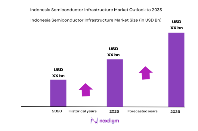
Indonesia semiconductor infrastructure market is valued at approximately USD ~ billion based on a recent historical assessment, supported by verified semiconductor capital expenditure disclosures and national industrial investment records. The market is driven by assembly and test facility expansion, government backed electronics manufacturing zones, and multinational semiconductor supply chain relocation into Southeast Asia. Rising automotive electronics production and power semiconductor localization further accelerate fab utility, cleanroom, and packaging infrastructure investments across industrial estates.
Jakarta metropolitan region, Batam island, and West Java manufacturing corridors dominate Indonesia semiconductor infrastructure deployment due to established electronics clusters, export oriented free trade zones, and proximity to regional semiconductor logistics routes. Batam benefits from bonded manufacturing incentives and Singapore linked supply chains, while West Java hosts large scale electronics and automotive manufacturing ecosystems requiring packaging and test capacity. Government industrial park programs and reliable port connectivity reinforce infrastructure concentration in these provinces.
Market Segmentation
By Product Type
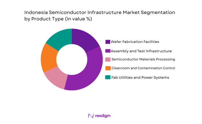
Indonesia Semiconductor Infrastructure market is segmented by product type into Wafer Fabrication Facilities, Assembly and Test Infrastructure, Semiconductor Materials Processing Systems, Cleanroom and Contamination Control Systems, and Fab Utilities and Power Systems. Recently, Assembly and Test Infrastructure has a dominant market share due to Indonesia’s positioning as a regional backend manufacturing hub, lower labor costs relative to wafer fabrication economies, established electronics export zones, and strong demand from automotive and consumer electronics supply chains seeking OSAT diversification. Government incentives and faster deployment timelines compared to front end fabs further reinforce dominance.
By Platform Type
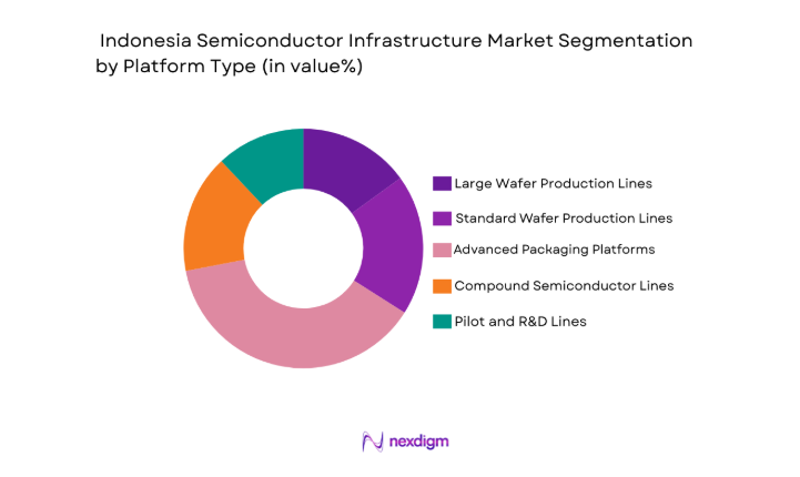
Indonesia Semiconductor Infrastructure market is segmented by platform type into Large Wafer Production Lines, Standard Wafer Production Lines, Advanced Packaging Platforms, Compound Semiconductor Lines, and Pilot and R&D Lines. Recently, Advanced Packaging Platforms has a dominant market share due to Indonesia’s rapid expansion in semiconductor assembly, testing, and packaging operations supporting automotive electronics and consumer devices, strong OSAT facility investments in Batam and West Java clusters, and regional semiconductor supply chain diversification favoring backend capacity growth over capital intensive front end wafer fabrication deployment.
Competitive Landscape
Indonesia semiconductor infrastructure market exhibits moderate consolidation with global semiconductor equipment suppliers and industrial infrastructure engineering firms dominating large scale projects, while regional contractors and utilities providers support localized deployment. Major players influence technology standards, fab design integration, and advanced packaging infrastructure through turnkey solutions and partnerships with multinational semiconductor manufacturers entering Indonesia.
| Company Name | Establishment Year | Headquarters | Technology Focus | Market Reach | Key Products | Revenue | Indonesia Project Capability |
| Applied Materials | 1967 | USA | ~ | ~ | ~ | ~ | ~ |
| Lam Research | 1980 | USA | ~ | ~ | ~ | ~ | ~ |
| Tokyo Electron | 1963 | Japan | ~ | ~ | ~ | ~ | ~ |
| ASM International | 1968 | Netherlands | ~ | ~ | ~ | ~ | ~ |
| ULVAC | 1952 | Japan | ~ | ~ | ~ | ~ | ~ |
Indonesia Semiconductor Infrastructure Market Analysis
Growth Drivers
Government Led Semiconductor Industrialization and Incentive Programs
Indonesia’s semiconductor infrastructure expansion is strongly supported by national electronics and semiconductor industrialization strategies that prioritize downstream manufacturing value addition, industrial diversification, and supply chain resilience, resulting in large scale industrial estate development and targeted fiscal incentives for semiconductor backend and materials facilities. Public investment in bonded logistics zones, tax holidays for high technology manufacturing, and accelerated permitting frameworks reduces project risk for multinational semiconductor firms considering Indonesia as an alternative to saturated East Asian backend hubs, while infrastructure co funding in utilities, water treatment, and cleanroom ready land parcels lowers entry barriers for assembly and packaging investors. Automotive electrification growth across ASEAN significantly increases regional demand for power semiconductor packaging and test services, encouraging OSAT firms to establish new Indonesian capacity near automotive manufacturing clusters to reduce logistics costs and supply risk. Electronics manufacturing relocation from China toward Southeast Asia due to trade diversification strategies further drives semiconductor packaging and test infrastructure investment, with Indonesia benefiting from scale advantages in land availability and labor cost competitiveness relative to neighboring economies. Rising domestic electronics consumption including consumer appliances, smartphones, and automotive electronics supports local semiconductor backend capacity requirements, improving project viability for multinational firms evaluating Indonesia infrastructure deployment. Integration of Indonesia into regional semiconductor supply chains anchored by Singapore, Malaysia, and Taiwan enhances attractiveness of Indonesian assembly and test infrastructure as a complementary node rather than a standalone fab ecosystem. Government collaboration with foreign semiconductor firms through joint industrial parks and technology partnerships further accelerates infrastructure development timelines by aligning regulatory, land, and utilities provisioning with investor requirements. Long term policy signaling around semiconductor industrial clusters provides investment certainty that encourages infrastructure financing institutions and industrial developers to commit capital to cleanroom ready facilities and semiconductor grade utilities networks.
Global Semiconductor Supply Chain Diversification Toward Southeast Asia
Structural shifts in semiconductor manufacturing geography driven by geopolitical risk management, trade resilience strategies, and cost optimization are redirecting backend semiconductor infrastructure investment toward Southeast Asia, positioning Indonesia as an emerging node due to its scale advantages and policy support for electronics manufacturing expansion. Multinational semiconductor firms seek geographic redundancy for assembly and test operations to mitigate concentration risk in traditional hubs, and Indonesia offers competitive industrial land pricing, labor availability, and improving logistics connectivity that collectively reduce lifecycle infrastructure costs for OSAT facilities. Regional automotive semiconductor demand growth associated with electrification and advanced driver systems increases need for diversified packaging and testing capacity across ASEAN, encouraging suppliers to deploy infrastructure closer to automotive production bases including Indonesia. Electronics contract manufacturing migration from China into Indonesia manufacturing corridors creates downstream demand for semiconductor packaging services, reinforcing local infrastructure investments in cleanrooms, materials handling, and process utilities. Comparative analysis of operating cost structures across Asia shows Indonesia maintaining favorable cost positioning for backend operations relative to developed semiconductor economies, enhancing investor interest in assembly and test infrastructure deployment. Government backed industrial park ecosystems integrating electronics manufacturing and semiconductor backend facilities improve supply chain efficiency and shorten production cycles for multinational firms. Cross border semiconductor logistics flows through Singapore and Malaysia provide Indonesia connectivity into established semiconductor trade networks, reducing perceived infrastructure isolation risks. Continued global semiconductor demand expansion across automotive, power electronics, and industrial sectors sustains long term requirement for diversified backend capacity, supporting sustained Indonesian semiconductor infrastructure development momentum.
Market Challenges
Limited Domestic Semiconductor Engineering and Technical Workforce Depth
Indonesia semiconductor infrastructure development faces structural constraints arising from limited availability of specialized semiconductor engineering, process integration, and advanced manufacturing technical skills required to design, install, and operate high precision cleanroom and semiconductor utility systems. Dependence on expatriate engineers and foreign technical contractors increases project costs and lengthens infrastructure deployment timelines, reducing competitiveness relative to mature semiconductor ecosystems with established technical talent pools. Training pipelines in semiconductor process engineering, contamination control, and fab facility management remain nascent within Indonesia’s industrial education system, constraining scalability of domestic semiconductor infrastructure operations. Technology transfer from multinational semiconductor firms into local engineering firms progresses gradually due to intellectual property sensitivities and complexity of semiconductor manufacturing knowhow, limiting domestic capability accumulation in advanced infrastructure design and maintenance. Limited experience among local contractors in semiconductor grade utilities such as ultra pure water systems, specialty gas handling, and vibration controlled cleanroom construction increases reliance on foreign EPC providers, raising infrastructure capital intensity. Workforce mobility constraints across Indonesian islands and industrial regions further complicate deployment of specialized semiconductor infrastructure teams to emerging industrial parks. Absence of large scale operational semiconductor fabs historically reduces domestic experiential learning opportunities that typically build engineering ecosystems around semiconductor clusters. Without accelerated investment in semiconductor technical education and industry training partnerships, infrastructure deployment scalability may remain constrained despite policy incentives and investor interest.
Infrastructure Quality Gaps in Power Reliability and Semiconductor Grade Utilities
Semiconductor manufacturing infrastructure requires exceptionally stable power supply, ultra pure water availability, contamination free air systems, and precision environmental control, yet several Indonesian industrial regions still face gaps in utility reliability and semiconductor grade infrastructure standards necessary for advanced manufacturing operations. Power grid fluctuations, localized outages, and voltage instability in certain industrial zones increase risk for sensitive semiconductor equipment and require costly redundant power and conditioning systems that elevate project capital expenditure. Water purification and wastewater treatment infrastructure capable of meeting semiconductor grade specifications remains limited outside major industrial estates, constraining site selection flexibility for new semiconductor facilities. Industrial gas supply chains for specialty semiconductor gases such as nitrogen, argon, and process chemicals are still developing domestically, increasing import dependence and logistics complexity for infrastructure deployment. Environmental control requirements including vibration isolation, particulate filtration, and humidity stability demand specialized construction capabilities not uniformly available across Indonesian industrial contractors. Geographic dispersion of Indonesian islands creates logistical challenges for transporting large semiconductor infrastructure equipment and materials, lengthening installation schedules. Infrastructure certification and regulatory compliance frameworks for semiconductor facilities remain evolving, adding administrative uncertainty to project development. Addressing semiconductor grade infrastructure gaps requires sustained investment in utilities modernization and industrial ecosystem integration, without which Indonesia may remain concentrated in lower complexity backend operations.
Opportunities
Development of Regional Advanced Packaging and Automotive Semiconductor Hub
Indonesia has a significant opportunity to establish itself as a regional advanced packaging and automotive semiconductor infrastructure hub by leveraging proximity to ASEAN automotive manufacturing clusters, growing electric vehicle production, and increasing demand for power and sensor semiconductor packaging within Southeast Asia supply chains. Automotive electrification significantly increases semiconductor content per vehicle, driving demand for packaging, test, and reliability infrastructure capable of handling power devices and automotive grade components that can be competitively located in Indonesia near vehicle manufacturing bases. Integration of semiconductor backend facilities with automotive electronics manufacturing ecosystems in West Java and surrounding industrial corridors enables supply chain efficiency and cost optimization for multinational automotive suppliers. Government incentives targeting electric vehicle supply chains align with semiconductor packaging infrastructure requirements, encouraging co location of automotive semiconductor facilities with battery and vehicle manufacturing plants. Regional automotive manufacturers seeking supply resilience increasingly prefer geographically diversified semiconductor packaging capacity, creating market pull for Indonesian infrastructure investment. Collaboration with established OSAT firms and automotive semiconductor suppliers can accelerate technology transfer into Indonesia packaging ecosystems. Industrial park developers can create specialized automotive semiconductor clusters integrating testing, reliability labs, and cleanroom facilities to attract global semiconductor firms. By positioning as an automotive semiconductor packaging hub, Indonesia can capture high growth segments of semiconductor infrastructure demand linked to mobility electrification trends.
Localization of Compound Semiconductor and Power Electronics Infrastructure
Indonesia possesses favorable conditions to develop compound semiconductor and power electronics infrastructure supporting renewable energy, electrification, and industrial power applications across Southeast Asia, given increasing regional demand for silicon carbide and gallium nitride devices in energy conversion and mobility systems. Renewable energy expansion and grid modernization initiatives across ASEAN increase need for power semiconductor modules, creating downstream demand for packaging and materials infrastructure that Indonesia can localize within industrial zones. Compound semiconductor manufacturing typically requires lower scale and investment intensity compared to advanced logic fabs, making it suitable for emerging semiconductor economies seeking entry into higher value semiconductor segments. Indonesia’s growing electric vehicle ecosystem and power electronics manufacturing demand create domestic anchor markets for compound semiconductor packaging and module infrastructure deployment. Strategic partnerships with global compound semiconductor firms can facilitate technology transfer and accelerate domestic capability development in epitaxy, materials processing, and packaging. Industrial policy support for clean energy technologies aligns with compound semiconductor infrastructure investment priorities, enabling integrated semiconductor energy technology clusters. Localization of power electronics infrastructure reduces import dependence for renewable energy and mobility systems while enhancing supply chain resilience. By focusing on compound semiconductor infrastructure, Indonesia can move beyond traditional assembly operations toward higher technology semiconductor manufacturing segments.
Future Outlook
Indonesia semiconductor infrastructure market is expected to expand steadily as Southeast Asian semiconductor supply chain diversification accelerates and domestic electronics manufacturing scales. Advanced packaging, automotive semiconductor, and power electronics infrastructure investments are likely to drive capacity additions across industrial corridors. Government incentives and industrial park development will improve utilities readiness and attract multinational semiconductor firms. Technology partnerships and workforce development programs are expected to strengthen domestic semiconductor infrastructure capabilities over the next five years.
Major Players
- Applied Materials
- Lam Research
- Tokyo Electron
- ASM International
- ULVAC
- SCREEN Semiconductor Solutions
- KLA Corporation
- Hitachi High-Tech
- Advantest
- Teradyne
- Entegris
- Air Liquide Electronics
- Linde Engineering
- NAURA Technology Group
- ASML
Key Target Audience
- Semiconductor manufacturers
- Electronics manufacturing companies
- Automotive electronics producers
- Industrial park developers
- Equipment suppliers
- Investments and venture capitalist firms
- Government and regulatory bodies
- Industrial infrastructure developers
Research Methodology
Step 1: Identification of Key Variables
Key infrastructure categories, semiconductor value chain stages, investment flows, and end user demand drivers were mapped across Indonesian semiconductor industrial zones. Supply chain linkages and technology segments were identified through industry databases and investment disclosures.
Step 2: Market Analysis and Construction
Market size and segmentation were constructed using capital expenditure benchmarks, facility counts, and semiconductor infrastructure cost models. Regional industrial deployment patterns and end user demand mapping informed segment shares and structure.
Step 3: Hypothesis Validation and Expert Consultation
Assumptions regarding infrastructure demand drivers, segment dominance, and growth dynamics were validated through consultations with semiconductor equipment suppliers, industrial developers, and regional electronics manufacturers.
Step 4: Research Synthesis and Final Output
Validated quantitative and qualitative insights were synthesized into market sizing, segmentation, competitive landscape, and strategic analysis frameworks. Outputs were structured into standardized semiconductor infrastructure market reporting format.
- Executive Summary
- Research Methodology (Definitions, Scope, Industry Assumptions, Market Sizing Approach, Primary & Secondary Research Framework, Data Collection & Verification Protocol, Analytic Models & Forecast Methodology, Limitations & Research Validity Checks)
- Market Definition and Scope
- Value Chain & Stakeholder Ecosystem
- Regulatory / Certification Landscape
- Sector Dynamics Affecting Demand
- Strategic Initiatives & Infrastructure Growth

- Growth Drivers
National semiconductor industrialization policies and incentives
Rising electronics manufacturing localization demand
Expansion of global semiconductor supply chain diversification
Growth in automotive and power semiconductor demand
Infrastructure investments in industrial parks and utilities - Market Challenges
High capital intensity and financing constraints
Limited domestic semiconductor engineering capabilities
Supply chain dependence on imported equipment
Infrastructure readiness gaps in power and water quality
Long gestation periods for fab project realization - Market Opportunities
Development of assembly and test hubs for regional supply chains
Localization of compound semiconductor production
Public private partnerships for fab infrastructure - Trends
Shift toward advanced packaging infrastructure
Integration of fab automation and smart manufacturing
Growth of power and analog semiconductor lines
Emergence of modular and scalable fab concepts
Increased environmental and resource efficiency requirements - Government Regulations & Defense Policy
Semiconductor investment incentives and tax benefits
Industrial land and utility provisioning policies
Technology transfer and foreign investment regulations - SWOT Analysis
- Stakeholder and Ecosystem Analysis
- Porter’s Five Forces Analysis
- Competition Intensity and Ecosystem Mapping
- By Market Value, 2020-2025
- By Installed Units, 2020-2025
- By Average System Price, 2020-2025
- By System Complexity Tier, 2020-2025
- By System Type (In Value%)
Wafer Fabrication Facilities
Assembly and Test Infrastructure
Semiconductor Materials Processing Systems
Cleanroom and Contamination Control Systems
Power and Utility Infrastructure for Fab - By Platform Type (In Value%)
Large Wafer Production Lines
Standard Wafer Production Lines
Advanced Packaging Platforms
Compound Semiconductor Lines
Pilot and R&D Lines - By Fitment Type (In Value%)
Greenfield Fab Installations
Brownfield Capacity Expansions
Modular Fab Units
Retrofit and Upgrade Systems
Turnkey Integrated Fab Solutions - By EndUser Segment (In Value%)
Integrated Device Manufacturers
Outsourced Semiconductor Assembly and Test Providers
Foundry Operators
Electronics Manufacturing Services Firms
Government and Research Institutes - By Procurement Channel (In Value%)
Direct OEM Procurement
EPC and Turnkey Contractors
Government Incentive Programs
Strategic Joint Ventures
Technology Transfer Partnerships - By Material / Technology (in Value %)
Silicon Wafer Processing Technologies
Compound Semiconductor Materials Infrastructure
Advanced Lithography Enablement Systems
Ultra Pure Water and Chemical Handling Systems
Fab Automation and Robotics Technologies
- Market structure and competitive positioning
Market share snapshot of major players - Cross Comparison Parameters (Technology Node Capability, Fab Capacity Scale, Infrastructure Integration Scope, Localization Level, Partnership Models)
- SWOT Analysis of Key Competitors
- Pricing & Procurement Analysis
- Key Players
Applied Materials
ASML
Lam Research
Tokyo Electron
KLA Corporation
Advantest
ASM International
SCREEN Semiconductor Solutions
Hitachi High-Tech
ULVAC
Teradyne
Entegris
Air Liquide Electronics
Linde Engineering
Beijing NAURA Technology Group
- Integrated device manufacturers prioritizing local capacity resilience
- OSAT providers expanding regional assembly capabilities
- Foundries targeting specialty and mature node production
- Government institutes supporting R&D and pilot fabrication
- Forecast Market Value, 2026-2035
- Forecast Installed Units, 2026-2035
- Price Forecast by System Tier, 2026-2035
- Future Demand by Platform, 2026-2035


 Request a Sample
 Ask for Customization
 Get a Quote
 Enquire Now