
 Download PDF
 Download PDF
Market Overview
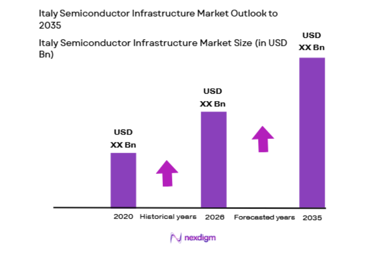
Italy’s semiconductor infrastructure market reached approximately USD ~ billion based on a recent historical assessment, supported by sustained capital deployment into wafer fabrication facilities, assembly and test capacity, and specialty materials ecosystems. Growth is driven by EU semiconductor sovereignty programs, automotive electronics demand, and analog-mixed signal manufacturing strengths. Public funding through the EU Chips Act and Italy’s national microelectronics incentives accelerated investments in cleanroom expansion, lithography tooling, and advanced packaging facilities across established industrial clusters.
Northern Italy dominates semiconductor infrastructure activity, particularly in Lombardy, Piedmont, and Emilia-Romagna, where established electronics manufacturing networks and automotive supply chains create persistent demand for fabrication and test capacity. Milan and Turin host major design centers, MEMS development, and equipment integration firms, supported by strong engineering universities and regional innovation grants.
Market Segmentation
By Product Type
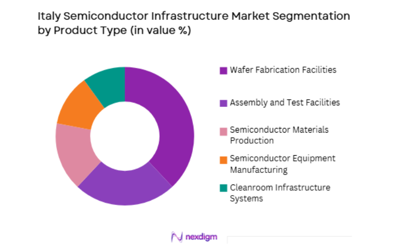
Italy Semiconductor Infrastructure market is segmented by product type into wafer fabrication facilities, assembly and test facilities, semiconductor materials production, semiconductor equipment manufacturing, and cleanroom infrastructure systems. Recently, wafer fabrication facilities has a dominant market share due to factors such as demand patterns, brand presence, infrastructure availability, or consumer preference.
By End-Use Industry
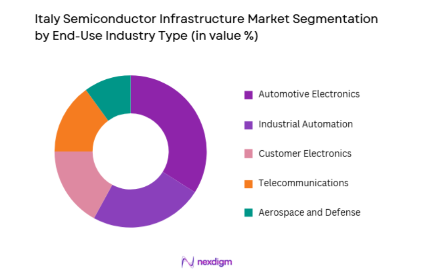
Italy Semiconductor Infrastructure market is segmented by end-use industry into automotive electronics, industrial automation, consumer electronics, telecommunications, and aerospace and defense. Recently, automotive electronics has a dominant market share due to factors such as demand patterns, brand presence, infrastructure availability, or consumer preference. Italy’s automotive manufacturing ecosystem and electrification transition have intensified domestic semiconductor sourcing needs, particularly for power devices, sensors, and control chips, encouraging localized infrastructure expansion and packaging capacity investments near automotive clusters.
Competitive Landscape
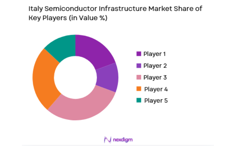
Italy’s semiconductor infrastructure market exhibits moderate consolidation, anchored by global integrated device manufacturers and specialized European materials and equipment firms with longstanding Italian operations. Multinational leaders leverage established fabs and R&D centers in northern regions, while domestic engineering and cleanroom specialists supply infrastructure systems. Strategic partnerships between device manufacturers, automotive OEMs, and public research institutions shape investment cycles and technology adoption, reinforcing cluster-based competition and barriers to entry in advanced manufacturing segments.
| Company Name | Establishment Year | Headquarters | Technology Focus | Market Reach | Key Products | Revenue | Italy Fab Presence |
| STMicroelectronics | 1987 | Geneva, Switzerland | ~ | ~ | ~ | ~ | ~ |
| Infineon Technologies | 1999 | Neubiberg, Germany | ~ | ~ | ~ | ~ | ~ |
| ASE Technology Holding | 1984 | Kaohsiung, Taiwan | ~ | ~ | ~ | ~ | ~ |
| Applied Materials | 1967 | Santa Clara, USA | ~ | ~ | ~ | ~ | ~ |
| ASM International | 1968 | Almere, Netherlands | ~ | ~ | ~ | ~ | ~ |
Italy Semiconductor Infrastructure Market Analysis
Growth Drivers
European Semiconductor Sovereignty Funding and National Incentive Alignment
explanation continues in the same sentence. Italy’s semiconductor infrastructure expansion is strongly influenced by coordinated European and national policy frameworks designed to localize semiconductor production capacity and reduce external supply dependence across critical electronics value chains. Public funding streams under the EU Chips Act and complementary Italian industrial incentives have lowered capital risk for fab modernization, advanced packaging deployment, and materials ecosystem scaling, encouraging multinational semiconductor manufacturers to expand Italian operations rather than concentrating investment solely in larger European hubs. Regional authorities in Lombardy, Piedmont, and Emilia-Romagna have further supplemented national incentives with tax credits, land grants, and infrastructure subsidies targeted at cleanroom construction and advanced process tool installation, creating geographically concentrated semiconductor clusters with high supplier density. This funding alignment has accelerated adoption of silicon carbide and power semiconductor fabrication infrastructure in Italy, particularly supporting automotive electrification supply chains that require localized wafer processing and packaging capacity near vehicle manufacturing plants. Public-private co-investment models involving device manufacturers, equipment suppliers, and research institutes have strengthened Italy’s capability in specialty process technologies such as MEMS and analog mixed-signal manufacturing, reinforcing the country’s niche advantages within the European semiconductor landscape. The predictable multiyear funding visibility associated with EU industrial policy has improved investment planning horizons for semiconductor firms, enabling phased expansion of fabs, materials plants, and testing facilities rather than sporadic capacity additions driven solely by market cycles.
Automotive Electrification and Power Semiconductor Localization Demand
explanation continues in the same sentence. Italy’s role within Europe’s automotive manufacturing network is generating sustained demand for domestic semiconductor infrastructure, particularly for power devices, sensors, and control electronics essential to electrified vehicle architectures and advanced driver systems. Electrification transitions across passenger and commercial vehicle segments have sharply increased consumption of silicon carbide and power management semiconductors, encouraging manufacturers to expand wafer fabrication and packaging capacity closer to automotive production clusters in northern Italy. Automotive OEM requirements for supply security and reduced logistics risk have driven long-term sourcing agreements with semiconductor suppliers operating Italian facilities, creating stable utilization expectations that justify infrastructure expansion investments. Italy’s established competence in power electronics engineering and automotive component manufacturing has reinforced the attractiveness of localized semiconductor fabrication for traction inverters, battery management systems, and charging electronics that require specialized process technologies. Collaborative R&D initiatives between semiconductor firms and automotive manufacturers in Turin and surrounding industrial districts are accelerating co-development of next-generation power devices, necessitating pilot fabrication lines and advanced packaging infrastructure within Italy.
Market Challenges
High Capital Intensity and Scale Constraints in Advanced Semiconductor Manufacturing
Explanation continues in the same sentence. Semiconductor infrastructure deployment in Italy faces structural challenges arising from the extremely high capital requirements and scale economics associated with modern fabrication facilities, which often favor concentration in a limited number of global mega-fabs rather than distributed regional capacity. Italy’s semiconductor ecosystem is historically oriented toward specialty and power devices rather than leading-edge logic manufacturing, limiting the country’s ability to attract the largest capital investments required for sub-10-nanometer process nodes and advanced lithography infrastructure.
Skilled Workforce Availability and Advanced Process Expertise Gaps
Italy’s semiconductor infrastructure growth is constrained by the limited availability of highly specialized engineering talent required for advanced fabrication, process integration, and semiconductor equipment operation, particularly in emerging domains such as silicon carbide processing and advanced packaging technologies. Semiconductor manufacturing demands multidisciplinary expertise across materials science, microelectronics, chemical engineering, and precision automation, and Italy’s talent pipeline in these fields is smaller compared to major semiconductor manufacturing regions in Asia and parts of northern Europe. Competition for experienced semiconductor engineers within Europe has intensified as multiple countries expand domestic fabrication capacity under strategic autonomy initiatives, making talent attraction and retention a significant constraint for Italian semiconductor facilities. Training new semiconductor specialists requires long lead times due to the complexity of fabrication processes and the need for hands-on experience in cleanroom environments, slowing workforce scaling relative to infrastructure investment ambitions. Universities and technical institutes in Italy provide strong electronics and engineering education, but alignment between academic programs and semiconductor manufacturing skill requirements remains uneven, creating gaps in advanced process expertise needed for next-generation infrastructure.
Opportunities
Silicon Carbide and Wide-Bandgap Semiconductor Manufacturing Expansion
Italy holds a strategic opportunity to expand semiconductor infrastructure through specialization in silicon carbide and other wide-bandgap semiconductor technologies that are experiencing rapid demand growth across electrified transport, renewable energy systems, and industrial power electronics applications. European electrification policies and energy transition initiatives are increasing consumption of high-efficiency power semiconductors, creating sustained market demand for silicon carbide wafer processing and device fabrication capacity that aligns with Italy’s established strengths in power electronics engineering. Italian semiconductor firms and research institutions already possess technical capabilities in wide-bandgap materials and device design, providing a foundation for scaling fabrication infrastructure without competing directly in leading-edge logic manufacturing dominated by global mega-fabs. Localization of silicon carbide wafer production and device packaging within Italy can reduce supply chain dependence on external sources while supporting European automotive and industrial manufacturers requiring reliable power semiconductor supply.
Advanced Packaging and Heterogeneous Integration Infrastructure Development
The global semiconductor industry’s transition toward advanced packaging and heterogeneous integration architectures creates a significant opportunity for Italy to expand semiconductor infrastructure in assembly, test, and integration segments that require lower capital intensity than leading-edge wafer fabrication. Advanced packaging technologies such as system-in-package, wafer-level packaging, and chiplet integration are increasingly essential for performance scaling in automotive, industrial, and communications electronics, sectors where Italy already has strong manufacturing presence. Collaboration between semiconductor device manufacturers, materials suppliers, and equipment firms in Italy can accelerate adoption of heterogeneous integration processes requiring specialized packaging infrastructure.
Future Outlook
Italy’s semiconductor infrastructure market is expected to expand steadily over the next five years, supported by European semiconductor sovereignty initiatives, automotive electrification demand, and specialization in power and sensor technologies. Continued public funding and regional industrial policies will sustain fab modernization and advanced packaging deployment. Technological shifts toward silicon carbide and heterogeneous integration will shape investment priorities.
Major Players
- STMicroelectronics
- Infineon Technologies
- ASE Technology Holding
- Applied Materials
- ASM International
- Soitec
- GlobalFoundries
- Bosch Semiconductor
- Tokyo Electron
- Lam Research
- ASML
- KLA Corporation
- Linde plc
- Air Liquide
- Merck KGaA
Key Target Audience
- Semiconductor device manufacturers
- Automotive OEMs
- Electronics manufacturing companies
- Industrial automation firms
- Telecommunications equipment providers
- Investments and venture capitalist firms
- Government and regulatory bodies
- Semiconductor equipment suppliers
Research Methodology
Step 1: Identification of Key Variables
Core variables including semiconductor fabrication capacity, packaging infrastructure, materials supply chains, and end-use demand sectors were defined. Regional policy incentives, automotive production activity, and semiconductor technology specialization factors were mapped to assess infrastructure drivers.
Step 2: Market Analysis and Construction
Primary and secondary data from industry associations, corporate disclosures, and policy programs were synthesized to construct Italy’s semiconductor infrastructure value chain. Segment shares and competitive positioning were derived through triangulation of facility capacity, investment activity, and technology focus.
Step 3: Hypothesis Validation and Expert Consultation
Infrastructure growth assumptions and segment dominance patterns were validated through consultation with semiconductor manufacturing experts and engineering specialists. Cross-verification ensured alignment with observed investment cycles and regional industrial dynamics.
Step 4: Research Synthesis and Final Output
Validated data and qualitative insights were integrated into a structured market framework covering segmentation, competition, drivers, challenges, and opportunities. Final outputs were reviewed for consistency with semiconductor industry economics and Italy’s regional manufacturing structure.
- Executive Summary
- Research Methodology (Definitions, Scope, Industry Assumptions, Market Sizing Approach, Primary & Secondary Research Framework, Data Collection & Verification Protocol, Analytic Models & Forecast Methodology, Limitations & Research Validity Checks)
- Market Definition and Scope
- Value Chain & Stakeholder Ecosystem
- Regulatory / Certification Landscape
- Sector Dynamics Affecting Demand

- Growth Drivers
European semiconductor sovereignty and fab investment programs
Automotive and industrial semiconductor demand growth
Expansion of advanced packaging capacity in Europe - Market Challenges
High capital requirements for semiconductor fabs
Dependence on imported advanced equipment and materials
Complex regulatory and environmental compliance - Market Opportunities
Development of advanced packaging and test hubs
Public private semiconductor fab initiatives
Growth in specialty and mature node production - Trends
Automation and smart manufacturing in semiconductor fabs
Shift toward heterogeneous integration and advanced packaging - Government Regulations
- SWOT Analysis
- Porter’s Five Forces
- By Market Value, 2020-2025
- By Installed Units, 2020-2025
- By Average System Price, 2020-2025
- By System Complexity Tier, 2020-2025
- By System Type (In Value%)
Wafer Fabrication Equipment
Semiconductor Assembly and Packaging Equipment
Semiconductor Testing and Metrology Systems
Cleanroom and Fab Facility Infrastructure
Semiconductor Materials Handling Systems - By Platform Type (In Value%)
Front End Wafer Fabrication Facilities
Back End Assembly and Packaging Facilities
Semiconductor R&D and Pilot Lines
Specialty Semiconductor Fabs
Outsourced Semiconductor Manufacturing Facilities - By Fitment Type (In Value%)
New Semiconductor Fab Construction
Fab Expansion and Retrofit Projects
Modular Cleanroom Installations
Integrated Fab Infrastructure Solutions - By End User Segment (In Value%)
Integrated Device Manufacturers
Outsourced Semiconductor Assembly and Test Providers
Research Institutes and Universities
- Market Share Analysis
- Cross Comparison Parameters (Process Node Capability, Fab Scale, Automation Level, Yield Efficiency, Packaging Technology, Equipment Sophistication, Cleanroom Class, Throughput Capacity, Energy Efficiency, Materials Handling Automation, Technology Maturity, Capex Intensity)
- SWOT Analysis of Key Competitors
- Pricing & Procurement Analysis
- Key Players
ASML
Applied Materials
Lam Research
KLA Corporation
Tokyo Electron
SCREEN Semiconductor Solutions
ASM International
Teradyne
Advantest
STMicroelectronics
Infineon Technologies
Intel
GlobalFoundries
Amkor Technology
ASE Technology
- IDMs investing in European semiconductor capacity
- OSAT providers expanding packaging and test operations
- Research institutes strengthening semiconductor R&D
- Manufacturers seeking regional chip supply resilience
- Forecast Market Value, 2026-2035
- Forecast Installed Units, 2026-2035
- Price Forecast by System Tier, 2026-2035
- Future Demand by Platform, 2026-2035


 Request a Sample
 Ask for Customization
 Get a Quote
 Enquire Now