
 Download PDF
 Download PDF
Market Overview
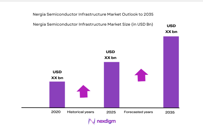
Nigeria semiconductor infrastructure market reached approximately USD ~ million based on a recent historical assessment, supported by government-led electronics manufacturing initiatives, telecommunications expansion, and rising data center investments. Capital deployment has focused on assembly, packaging, and testing facilities rather than wafer fabrication due to cost constraints. Infrastructure spending has also been driven by import substitution policies and regional supply chain resilience goals promoted by national industrial development programs and international technology partnerships.
Lagos and Ogun industrial corridors dominate Nigeria semiconductor infrastructure market due to established manufacturing ecosystems, port connectivity, and proximity to electronics assembly clusters. Abuja has emerged as a policy and research hub through federal technology programs and public semiconductor initiatives. Cross-border collaboration with Asian semiconductor economies influences infrastructure localization strategies, while southern coastal regions attract investment because of energy availability, logistics access, and concentration of private electronics manufacturers and telecom equipment assemblers.
Market Segmentation
By Product Type
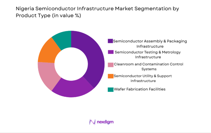
Nigeria semiconductor infrastructure market is segmented by product type into wafer fabrication infrastructure, semiconductor assembly and packaging infrastructure, semiconductor testing and metrology infrastructure, cleanroom and contamination control systems, and semiconductor utility and support infrastructure. Recently, semiconductor assembly and packaging infrastructure has a dominant market share due to factors such as demand patterns, brand presence, infrastructure availability, or consumer preference. The country’s semiconductor ecosystem is currently oriented toward downstream manufacturing and electronics assembly rather than capital-intensive wafer fabrication, creating stronger immediate demand for packaging and test capacity. Growth in telecom equipment assembly, consumer electronics manufacturing, and automotive electronics imports has increased the need for localized packaging to reduce lead times and logistics costs. Government industrial diversification programs prioritize value-added manufacturing stages that require lower capital thresholds than front-end fabs, further strengthening this segment. Availability of skilled technical labor in electronics assembly and the presence of contract manufacturing firms in Lagos and Ogun also support packaging infrastructure adoption. International semiconductor firms exploring African supply chains prefer assembly and testing partnerships before fabrication investment, reinforcing segment leadership.
By Platform Type
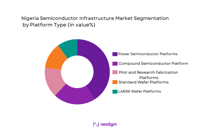
Nigeria semiconductor infrastructure market is segmented by platform type into Standard wafer platforms, Large wafer platforms, compound semiconductor platforms, advanced packaging platforms, and pilot and research fabrication platforms. Recently, advanced packaging platforms has a dominant market share due to factors such as demand patterns, brand presence, infrastructure availability, or consumer preference. Nigeria’s semiconductor activity is concentrated in back-end processes such as packaging, assembly, and integration for telecommunications devices, power electronics modules, and consumer electronics components, making advanced packaging platforms commercially viable. Domestic electronics manufacturers require system-in-package and module-level integration rather than full wafer processing capability, driving adoption of these platforms. Government technology programs and foreign partnerships emphasize modular packaging facilities that can be scaled gradually without full fabrication investment. The rise of power management and radio-frequency components in telecom and renewable energy applications also increases reliance on advanced packaging technologies. Limited availability of high-precision lithography and fabrication expertise further shifts infrastructure demand toward packaging-focused platforms in the national semiconductor ecosystem.
Competitive Landscape
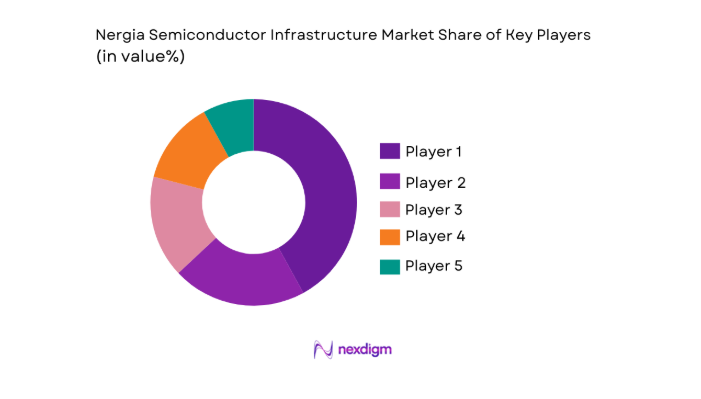
Nigeria semiconductor infrastructure market remains moderately consolidated with global semiconductor equipment manufacturers and infrastructure integrators supplying most advanced systems while domestic firms participate in assembly and facility integration. International technology providers influence standards, equipment sourcing, and facility design through partnerships and EPC contracts. Local participation is concentrated in packaging facilities, cleanroom installation, and utilities integration, while multinational semiconductor infrastructure vendors maintain technological leadership and regional supply relationships.
| Company Name | Establishment Year | Headquarters | Technology Focus | Market Reach | Key Products | Revenue | Semiconductor Infrastructure Role |
| ASML Holding | 1984 | Netherlands | ~ | ~ | ~ | ~ | ~ |
| Applied Materials | 1967 | USA | ~ | ~ | ~ | ~ | ~ |
| Lam Research | 1980 | USA | ~ | ~ | ~ | ~ | ~ |
| Tokyo Electron | 1963 | Japan | ~ | ~ | ~ | ~ | ~ |
| KLA Corporation | 1975 | USA | ~ | ~ | ~ | ~ | ~ |
Nigeria Semiconductor Infrastructure Market Analysis
Growth Drivers
Expansion of Electronics Manufacturing and Assembly Ecosystem
Nigeria’s expanding telecommunications equipment assembly, consumer electronics production, and power electronics integration industries are significantly increasing demand for semiconductor infrastructure, particularly in packaging, testing, and cleanroom systems, as manufacturers require localized semiconductor component processing to reduce import dependence and logistics delays while strengthening domestic value addition. The growth of mobile device assembly, broadcast equipment manufacturing, and solar inverter electronics production is creating consistent requirements for semiconductor packaging and module integration facilities across major industrial corridors. Domestic electronics firms are increasingly shifting toward partial localization of semiconductor integration processes to improve supply stability and cost control, reinforcing infrastructure investment momentum. The presence of contract manufacturing firms and electronics assemblers in Lagos and Ogun is fostering cluster-based demand for shared semiconductor infrastructure such as testing labs and contamination-controlled environments. Regional export ambitions toward West African consumer and telecom equipment markets are encouraging manufacturers to establish localized semiconductor assembly capabilities within Nigeria. Increasing adoption of semiconductor-intensive technologies such as smart meters, telecom base stations, and renewable energy systems is further expanding demand for semiconductor integration infrastructure. Public and private industrial parks are incorporating semiconductor-compatible manufacturing zones, enabling co-location of electronics and semiconductor assembly activities. As electronics manufacturing output continues rising, semiconductor packaging and testing infrastructure is becoming a critical enabler of Nigeria’s industrial diversification and manufacturing competitiveness.
Government Industrial Diversification and Technology Localization Policies
Nigeria’s national industrialization strategies emphasizing import substitution, technology transfer, and domestic manufacturing capability development are accelerating semiconductor infrastructure investment by prioritizing downstream semiconductor activities such as assembly, packaging, and testing facilities that align with current industrial capacity and workforce readiness. Government programs supporting electronics manufacturing clusters, free trade zones, and high-technology industrial parks are facilitating infrastructure deployment by providing land, utilities, and investment incentives for semiconductor-related facilities. Policies encouraging foreign direct investment in advanced manufacturing are enabling partnerships between Nigerian firms and global semiconductor infrastructure providers, improving access to equipment and technical expertise. Technology localization initiatives are promoting gradual movement up the semiconductor value chain, beginning with packaging and module integration before fabrication capability. Public procurement preferences for locally assembled electronics are increasing demand for domestic semiconductor integration capacity across telecommunications, energy, and defense-related electronics sectors. Industrial financing schemes and development bank support mechanisms are improving capital access for semiconductor infrastructure projects, particularly in packaging and testing segments. National digital economy strategies are reinforcing semiconductor demand through expansion of telecommunications networks, data infrastructure, and electronic device deployment programs. Regulatory emphasis on local value addition in electronics supply chains is creating structural incentives for domestic semiconductor infrastructure development, strengthening long-term market growth drivers.
Market Challenges
High Capital Intensity and Financing Constraints in Semiconductor Facilities
Semiconductor infrastructure development in Nigeria faces significant financial barriers because even downstream facilities such as packaging, testing, and cleanroom systems require substantial upfront investment in precision equipment, contamination-controlled environments, and specialized utilities, while domestic capital markets and industrial financing frameworks remain limited in supporting long-term technology infrastructure projects. Investors perceive semiconductor facilities as high-risk due to long payback periods, technology obsolescence risks, and dependence on imported equipment, increasing financing costs and reducing project feasibility. Currency volatility and import dependency for semiconductor equipment further elevate capital expenditure and operating costs for facility developers. Limited availability of specialized infrastructure financing instruments such as technology infrastructure funds or semiconductor development grants constrains large-scale deployment of advanced facilities. Domestic banks often lack familiarity with semiconductor project risk profiles, resulting in conservative lending terms and collateral requirements. Infrastructure developers must rely heavily on foreign investment or development finance, which may involve lengthy approval processes and partnership complexities. High power reliability requirements and backup utility infrastructure further increase facility capital costs compared with general manufacturing plants. These financial constraints collectively slow the pace of semiconductor infrastructure expansion and limit Nigeria’s ability to scale beyond packaging-focused facilities.
Limited Technical Expertise and Supporting Industrial Ecosystem
Nigeria semiconductor infrastructure market development is constrained by shortages in highly specialized engineering skills, semiconductor process expertise, and supporting supply chains for materials, maintenance, and precision facility services, as the national semiconductor ecosystem remains in early stages compared with established Asian and global semiconductor manufacturing regions. Semiconductor packaging and testing operations require trained technicians, contamination control specialists, equipment maintenance engineers, and process integration experts, many of whom are scarce domestically. Dependence on foreign technical personnel increases operational costs and limits knowledge transfer speed within local firms. Absence of domestic suppliers for semiconductor chemicals, ultra-pure materials, and precision components forces facilities to rely on imports, increasing operational complexity and supply chain risk. Limited presence of semiconductor equipment service providers and calibration laboratories further constrains facility reliability and maintenance efficiency. Training programs in microelectronics and semiconductor engineering remain limited, slowing workforce development required for infrastructure scaling. Collaboration between academia and industry in semiconductor technology is still emerging, reducing innovation and localization capability. Supporting industrial ecosystems such as precision manufacturing, specialty gas supply, and advanced materials logistics remain underdeveloped. These ecosystem gaps collectively restrict Nigeria’s ability to expand semiconductor infrastructure beyond initial packaging and assembly stages.
Opportunities
Development of Regional Semiconductor Assembly and Test Hub
Nigeria possesses strong potential to evolve into a regional semiconductor assembly and testing hub serving West Africa due to its large electronics consumption market, established manufacturing clusters, logistics connectivity through major ports, and growing telecommunications and renewable energy equipment industries that require semiconductor integration and packaging capabilities. Neighboring African economies rely heavily on imported electronic devices and components, creating regional demand for localized semiconductor back-end processing that Nigeria can serve efficiently. Establishing large-scale assembly and testing facilities would reduce supply chain lead times for regional electronics manufacturers while enabling Nigeria to capture higher value within semiconductor supply chains. Regional trade agreements and economic integration frameworks support cross-border electronics and component trade, enhancing market access for Nigerian semiconductor facilities. International semiconductor firms seeking diversified geographic manufacturing bases are increasingly exploring emerging markets with strong regional demand, positioning Nigeria as a candidate for partnership-based assembly operations. Government industrial zones and free trade areas provide infrastructure platforms suitable for semiconductor packaging clusters. Workforce availability in electronics assembly provides a foundation for training expansion into semiconductor packaging skills. Developing hub-level infrastructure would stimulate supporting ecosystems including materials logistics, testing services, and semiconductor equipment maintenance.
Strategic Partnerships with Global Semiconductor Infrastructure Providers
Collaboration between Nigerian industrial stakeholders and global semiconductor equipment manufacturers, infrastructure integrators, and packaging technology firms presents a major opportunity to accelerate semiconductor infrastructure deployment through technology transfer, joint ventures, and localized facility development aligned with Nigeria’s industrial capability trajectory. Global semiconductor firms are increasingly pursuing regional supply chain diversification strategies to mitigate geographic concentration risks, creating openings for emerging markets to host downstream semiconductor activities. Partnerships can provide access to advanced packaging equipment, cleanroom design expertise, and operational best practices that would otherwise be difficult to develop domestically. Joint development programs can enable gradual technology localization while maintaining global quality standards required for semiconductor processing. Foreign partners benefit from market entry into Africa’s largest economy and regional electronics demand base, while Nigerian stakeholders gain capability and credibility. Public-private partnership frameworks and investment incentives can support co-financed semiconductor infrastructure projects with shared risk. Training and workforce development initiatives embedded within partnerships can accelerate skill transfer and ecosystem growth. Successful collaboration models can position Nigeria within global semiconductor value chains as a reliable back-end processing location.
Major Players
- ASML Holding
- Applied Materials
- Lam Research
- Tokyo Electron
- KLA Corporation
- ASM International
- GlobalFoundries
- STMicroelectronics
- Infineon Technologies
- Texas Instruments
- Tower Semiconductor
- Amkor Technology
- ASE Technology Holding
- JCET Group
- Samsung Electronics
Key Target Audience
- Semiconductor equipment manufacturers
- Electronics manufacturing companies
- Telecommunications equipment producers
- Automotive electronics suppliers
- Investments and venture capitalist firms
- Government and regulatory bodies
- Industrial infrastructure developer
- Power and utility solution providers
Research Methodology
Step 1: Identification of Key Variables
Core semiconductor infrastructure components, investment flows, facility types, and industry demand indicators were mapped. Variables included packaging capacity, cleanroom infrastructure, electronics manufacturing output, and industrial policy incentives influencing semiconductor infrastructure deployment across Nigeria.
Step 2: Market Analysis and Construction
Market size and segmentation were constructed using facility investment data, electronics manufacturing activity, and semiconductor supply chain participation. Infrastructure categories were defined across packaging, testing, cleanroom, and fabrication platforms to estimate relative market distribution.
Step 3: Hypothesis Validation and Expert Consultation
Findings were validated through industry expert perspectives, equipment supplier insights, and regional semiconductor infrastructure benchmarks. Technology adoption patterns and facility deployment feasibility were cross-checked against comparable emerging semiconductor ecosystems.
Step 4: Research Synthesis and Final Output
All validated inputs were synthesized into a structured market framework covering segmentation, competitive landscape, drivers, challenges, and opportunities. Outputs were aligned with semiconductor infrastructure value chain dynamics and Nigeria’s industrial development trajectory.
- Executive Summary
- Research Methodology (Definitions, Scope, Industry Assumptions, Market Sizing Approach, Primary & Secondary Research Framework, Data Collection & Verification Protocol, Analytic Models & Forecast Methodology, Limitations & Research Validity Checks)
- Market Definition and Scope
- Value Chain & Stakeholder Ecosystem
- Regulatory / Certification Landscape
- Sector Dynamics Affecting Demand
- Strategic Initiatives & Infrastructure Growth

- Growth Drivers
National digitalization and electronics manufacturing initiatives
Rising demand for localized semiconductor supply chains
Growth in telecommunications and data infrastructure sectors
Government incentives for high-tech industrial investment
Expansion of regional semiconductor collaboration programs - Market Challenges
High capital intensity of semiconductor fabrication facilities
Limited domestic technical workforce and expertise
Infrastructure reliability constraints in power and utilities
Dependence on imported equipment and materials
Regulatory and investment approval complexities - Market Opportunities
Development of semiconductor assembly and packaging hubs
Public-private partnerships in fab infrastructure projects
Regional export potential within West African markets - Trends
Shift toward modular and scalable fab facility designs
Adoption of energy-efficient cleanroom technologies
Growth of compound semiconductor applications
Integration of automation and smart manufacturing systems
Increased collaboration with global semiconductor firms - Government Regulations & Defense Policy
Industrial policy incentives for electronics manufacturing
Technology transfer and foreign investment frameworks
Standards for semiconductor facility environmental compliance - SWOT Analysis
- Stakeholder and Ecosystem Analysis
- Porter’s Five Forces Analysis
- Competition Intensity and Ecosystem Mapping
- By Market Value, 2020-2025
- By Installed Units, 2020-2025
- By Average System Price, 2020-2025
- By System Complexity Tier, 2020-2025
- By System Type (In Value%)
Wafer Fabrication Facilities
Semiconductor Assembly and Packaging Lines
Test and Metrology Infrastructure
Cleanroom and Environmental Control Systems
Power and Utility Management Systems - By Platform Type (In Value%)
200mm Wafer Platforms
300mm Wafer Platforms
Advanced Packaging Platforms
Compound Semiconductor Platforms
Pilot and R&D Fabrication Platforms - By Fitment Type (In Value%)
Greenfield Fab Installations
Brownfield Facility Upgrades
Modular Fab Units
Integrated Fab and Packaging Facilities
Mobile or Compact Production Units - By EndUser Segment (In Value%)
Integrated Device Manufacturers
Outsourced Semiconductor Assembly and Test Providers
Fabless Semiconductor Firms
Government and Research Institutes
Electronics Manufacturing Services Providers - By Procurement Channel (In Value%)
Direct OEM Procurement
Engineering Procurement Construction Contractors
Government Tender Programs
Technology Transfer Partnerships
Distributor and Integrator Networks - By Material / Technology (in Value %)
Silicon Wafer Processing Technologies
Compound Semiconductor Materials Infrastructure
Photolithography and Patterning Systems
Etch and Deposition Technologies
Advanced Packaging Materials Systems
- Market structure and competitive positioning
Market share snapshot of major players - Cross Comparison Parameters (Technology Node Capability, Fab Capacity Scale, Equipment Portfolio Breadth, Packaging Integration Level, Energy Efficiency, Automation Level, Regional Presence, Partnership Ecosystem, Cost Structure)
- SWOT Analysis of Key Competitors
- Pricing & Procurement Analysis
- Key Players
ASML Holding
Applied Materials
Lam Research
Tokyo Electron
KLA Corporation
ASM International
Taiwan Semiconductor Manufacturing Company
Samsung Electronics
Intel Corporation
GlobalFoundries
STMicroelectronics
Infineon Technologies
Texas Instruments
Tower Semiconductor
Semiconductor Manufacturing International Corporation
- Integrated manufacturers seek regional fabrication capability
- OSAT providers expand packaging and testing capacity
- Research institutes drive pilot semiconductor facilities
- EMS firms demand localized semiconductor component supply
- Forecast Market Value, 2026-2035
- Forecast Installed Units, 2026-2035
- Price Forecast by System Tier, 2026-2035
- Future Demand by Platform, 2026-2035


 Request a Sample
 Ask for Customization
 Get a Quote
 Enquire Now