
 Download PDF
 Download PDF
Market Overview
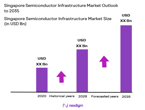
Based on a recent historical assessment, the Singapore Semiconductor Infrastructure market is valued at approximately USD ~ billion, supported by sustained capital expenditure across wafer fabrication, advanced packaging, and process utility systems. Investments from global foundries and equipment firms, alongside public incentives under Singapore’s manufacturing strategy, continue expanding cleanroom capacity, specialty gas distribution, and contamination control ecosystems. Infrastructure demand is further reinforced by advanced node transitions, heterogeneous integration adoption, and strong export-oriented semiconductor manufacturing activity.
Singapore remains a leading semiconductor infrastructure hub due to its concentration of high-value wafer fabrication and assembly operations in industrial clusters such as Tampines, Woodlands, and Pasir Ris, supported by advanced logistics and utilities reliability. The country’s dominance is reinforced by long-standing presence of multinational chipmakers, deep supplier ecosystems, and government-backed R&D platforms like A*STAR. Regional leadership is also sustained by proximity to Southeast Asian electronics manufacturing networks and stable regulatory and trade frameworks.
Market Segmentation
By Product Type
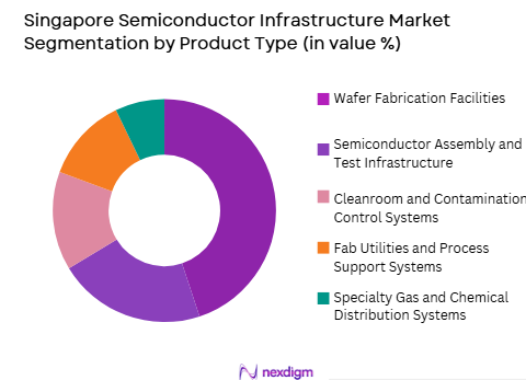
Singapore Semiconductor Infrastructure market is segmented by product type into wafer fabrication facilities, semiconductor assembly and test infrastructure, cleanroom and contamination control systems, fab utilities and process support systems, and specialty gas and chemical distribution systems. Recently, wafer fabrication facilities has a dominant market share due to factors such as sustained capital deployment by leading foundries, complex process node requirements, and large-scale cleanroom expansion programs. Singapore’s positioning as a global logic and specialty process manufacturing hub concentrates investments in front-end fabrication capacity rather than purely backend or ancillary infrastructure. The presence of multiple high-volume fabs drives demand for advanced lithography-ready cleanrooms, vibration-controlled substructures, and ultra-pure utility systems, reinforcing the segment’s scale leadership. Government incentives supporting advanced manufacturing upgrades and continuous fab modernization cycles further elevate fabrication infrastructure spending relative to other segments. Long project lifecycles and high asset intensity also contribute to higher cumulative value share within total semiconductor infrastructure expenditure in the country.
By Facility Type
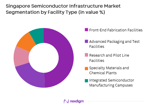
Singapore Semiconductor Infrastructure market is segmented by facility type into front-end fabrication facilities, advanced packaging and test facilities, research and pilot line facilities, specialty materials and chemical plants, and integrated semiconductor manufacturing campuses. Recently, front-end fabrication facilities has a dominant market share due to factors such as capital intensity, advanced node migration, and concentration of high-value manufacturing operations in Singapore. The country hosts multiple logic, analog, and specialty semiconductor fabs that require large-scale cleanroom shells, sub-fab utility systems, and high-purity distribution networks, driving infrastructure demand toward front-end operations. Compared with packaging or R&D facilities, fabrication plants involve significantly larger built-up areas, higher contamination control specifications, and more complex process support utilities, resulting in greater infrastructure spending. Strategic national policies supporting wafer fabrication resilience and supply chain security further prioritize front-end facility expansion over other facility types, sustaining its dominant share in semiconductor infrastructure investments.
Competitive Landscape
The Singapore Semiconductor Infrastructure market is moderately consolidated, with global engineering contractors, cleanroom specialists, and process utility providers competing alongside regional facility integrators. Large multinational semiconductor equipment and infrastructure firms dominate high-value fabrication and cleanroom projects, while local engineering firms support installation, retrofits, and lifecycle services. Strategic partnerships with foundries and government-supported R&D programs reinforce incumbents’ positions and create barriers to entry for smaller players.
| Company Name | Establishment Year | Headquarters | Technology Focus | Market Reach | Key Products | Revenue | Core Infrastructure Segment |
| Applied Materials | 1967 | United States | ~ | ~ | ~ | ~ | ~ |
| Lam Research | 1980 | United States | ~ | ~ | ~ | ~ | ~ |
| ASML | 1984 | Netherlands | ~ | ~ | ~ | ~ | ~ |
| Exyte | 1912 | Germany | ~ | ~ | ~ | ~ | ~ |
| Meissner | 1984 | United States | ~ | ~ | ~ | ~ | ~ |
Singapore Semiconductor Infrastructure Market Analysis
Growth Drivers
Advanced Node Migration and Fab Expansion Investments
Singapore’s semiconductor infrastructure growth is strongly driven by ongoing migration toward advanced and specialty semiconductor process nodes that require substantial upgrades to fabrication facilities and associated utilities. As semiconductor manufacturers transition toward smaller geometries and heterogeneous integration processes, infrastructure requirements become significantly more complex, demanding ultra-clean environments, vibration-controlled sub-structures, and high-precision temperature and humidity management systems. These technical requirements compel continuous reinvestment in cleanroom expansion, sub-fab utility networks, and advanced contamination control systems across existing facilities. Singapore’s role as a hub for analog, power, and specialty logic manufacturing further accelerates such infrastructure demand, as these segments increasingly adopt advanced packaging and integration techniques. Public sector support mechanisms and manufacturing transformation programs encourage global semiconductor firms to expand and modernize local fabrication capacity rather than relocate production. Long lifecycle investments in wafer fabrication plants create recurring infrastructure demand through phased expansions and equipment retrofits. The presence of established semiconductor clusters ensures that each fab expansion stimulates parallel growth in specialty gas distribution, chemical handling systems, and facility automation infrastructure. High export dependence of semiconductor manufacturing also incentivizes capacity upgrades to maintain technological competitiveness in global supply chains.
Government-Backed Semiconductor Manufacturing Ecosystem Development
Singapore’s semiconductor infrastructure market is also propelled by strong institutional support aimed at sustaining the country’s leadership in advanced manufacturing and electronics supply chains. National industrial strategies prioritize semiconductor fabrication resilience, advanced packaging capability, and process innovation capacity, leading to sustained public-private investment flows into semiconductor facilities and supporting infrastructure. Government agencies facilitate land allocation in specialized industrial zones, provide fiscal incentives for high-technology manufacturing upgrades, and co-fund R&D platforms that anchor global semiconductor firms locally. Such policy stability reduces investment risk for multinational manufacturers and encourages long-term facility commitments in Singapore. Public research institutions collaborate with industry on pilot lines and process development infrastructure, which indirectly drives demand for specialized cleanrooms and utilities. Workforce development initiatives ensure availability of skilled engineers and technicians capable of operating advanced semiconductor facilities, further strengthening the infrastructure ecosystem. Trade openness and regulatory predictability also attract semiconductor supply chain partners such as materials and chemical producers, expanding infrastructure needs beyond fabrication plants. Strategic positioning within Southeast Asian electronics manufacturing networks increases the importance of Singapore-based fabs, prompting continued capacity enhancement. Through coordinated industrial policy and infrastructure planning, Singapore sustains a high-value semiconductor manufacturing base that continually stimulates infrastructure expansion. This institutional ecosystem support therefore acts as a foundational long-term growth driver for semiconductor infrastructure investments.
Market Challenges
High Capital Intensity and Long Payback Periods in Semiconductor Facilities
Semiconductor infrastructure development in Singapore faces significant constraints due to the extremely high capital intensity associated with constructing and upgrading fabrication and advanced packaging facilities. Semiconductor fabs require multibillion-dollar investments in cleanroom shells, sub-fab utilities, and contamination control systems before any production equipment is installed, creating long payback horizons for investors. Such capital commitments expose manufacturers and infrastructure providers to cyclical semiconductor demand risks, potentially delaying expansion projects during market downturns. Infrastructure projects also involve highly specialized engineering and compliance requirements, increasing project complexity and cost overruns. The limited availability of land and rising construction costs in Singapore further elevate facility development expenditure relative to other manufacturing regions. High asset specificity reduces the flexibility of infrastructure investments, as semiconductor facilities cannot easily be repurposed for other industries. Financing constraints may arise for smaller infrastructure contractors lacking balance sheet strength to undertake large-scale semiconductor projects. Long construction and qualification timelines also delay revenue realization for facility developers and investors. Even when demand outlook is favorable, firms may adopt phased expansion strategies to mitigate financial risk, slowing infrastructure market growth. Consequently, capital intensity and investment risk remain persistent structural challenges affecting semiconductor infrastructure expansion in Singapore.
Space Constraints and Industrial Land Scarcity in a Dense Manufacturing Hub
Singapore’s semiconductor infrastructure market is also challenged by physical space limitations and industrial land scarcity within a highly urbanized national environment. Semiconductor fabrication plants require extensive cleanroom floor area, vibration-isolated foundations, and supporting utility zones, making them among the most space-intensive manufacturing facilities. However, Singapore’s limited land availability and competing industrial uses constrain opportunities for large-scale greenfield semiconductor facility development. Land allocation decisions must balance semiconductor manufacturing needs with logistics, energy, and other high-value industries, potentially restricting expansion pace. Vertical fab design and multi-story cleanroom configurations increase engineering complexity and infrastructure cost compared with conventional single-level fabs. Infrastructure retrofits within existing industrial estates may face zoning, utility capacity, or environmental constraints that limit upgrade feasibility. Expansion projects must also comply with strict environmental and safety regulations, particularly regarding chemical handling and waste treatment infrastructure. Rising land lease costs in prime industrial clusters further increase total semiconductor facility investment requirements. Manufacturers may therefore prioritize optimization of existing facilities rather than new builds, reducing incremental infrastructure demand. These spatial constraints structurally limit the scale and speed of semiconductor infrastructure growth despite strong industry demand drivers.
Opportunities
Advanced Packaging and Heterogeneous Integration Infrastructure Expansion
Singapore’s semiconductor infrastructure market has significant opportunity in supporting the global shift toward advanced packaging and heterogeneous integration technologies that complement traditional wafer fabrication. As semiconductor performance improvements increasingly rely on packaging innovations such as chiplet architectures and 3D integration, demand grows for specialized cleanrooms, precision assembly environments, and high-purity process utilities dedicated to packaging facilities. Singapore already hosts major assembly and test operations, positioning it to expand into higher-value advanced packaging infrastructure. Infrastructure requirements for advanced packaging involve distinct environmental controls, metrology support spaces, and chemical handling systems, creating new investment streams beyond conventional fabs. Global semiconductor firms are seeking geographically diversified packaging capabilities to enhance supply chain resilience, making Singapore an attractive expansion location. Public R&D initiatives in advanced packaging further stimulate pilot line and prototyping infrastructure development. Integration of packaging and fabrication within unified campuses increases demand for interconnected utility and logistics infrastructure. As heterogeneous integration becomes mainstream across electronics sectors, infrastructure spending intensity in packaging facilities rises significantly. Singapore’s engineering and manufacturing ecosystem can support such specialized facility development efficiently. Therefore, advanced packaging infrastructure represents a major future growth opportunity within the semiconductor infrastructure market.
Semiconductor Supply Chain Localization and Resilience Investments
Another major opportunity for Singapore semiconductor infrastructure arises from global efforts to strengthen supply chain resilience and regional manufacturing security in semiconductor production. Geopolitical tensions and supply disruptions have encouraged multinational semiconductor firms to diversify manufacturing footprints across stable and technologically advanced locations. Singapore’s political stability, strong intellectual property protection, and established semiconductor ecosystem make it a preferred site for resilient capacity expansion. Such strategic diversification drives new investments in fabrication upgrades, specialty materials plants, and supporting infrastructure networks within the country. Localization of critical semiconductor inputs such as specialty chemicals and gases further expands infrastructure demand in distribution and storage systems. Governments and corporations increasingly prioritize supply chain redundancy, leading to parallel infrastructure capacity rather than centralized mega-fabs. Singapore’s connectivity to global electronics manufacturing networks enhances its attractiveness for resilient semiconductor infrastructure deployment. Regional electronics growth in Southeast Asia also increases demand for nearby semiconductor production capacity. As supply chain security becomes a structural industry priority, infrastructure investments in stable hubs like Singapore accelerate. This resilience-driven localization trend therefore creates sustained long-term opportunities for semiconductor infrastructure expansion in the country.
Future Outlook
Over the next five years, Singapore Semiconductor Infrastructure market is expected to advance through continued fab modernization, advanced packaging expansion, and supply chain localization investments. Technological evolution toward heterogeneous integration and specialty semiconductor processes will increase infrastructure complexity and spending intensity per facility. Policy stability and ecosystem support will sustain multinational semiconductor commitments. However, land constraints and capital intensity will encourage vertical fab design, retrofits, and campus optimization strategies rather than extensive greenfield development.
Major Players
- Applied Materials
- Lam Research
- ASML
- Exyte
- Tokyo Electron
- KLA Corporation
- Linde Engineering
- Air Liquide Engineering
- Edwards Vacuum
- Daifuku
- Ultra Clean Holdings
- Entegris
- Hitachi High-Tech
- Merck Electronics
- GlobalFoundries
Key Target Audience
- Semiconductor manufacturers
- Advanced packaging companies
- Semiconductor equipment manufacturers
- Industrial infrastructure developers
- Specialty chemical and gas suppliers
- Investments and venture capitalist firms
- Government and regulatory bodies
- Electronics manufacturing conglomerates
Research Methodology
Step 1: Identification of Key Variables
Key semiconductor infrastructure variables including fabrication capacity, cleanroom space, utility intensity, and facility investment flows were identified across Singapore’s semiconductor clusters. Data inputs included manufacturing investment announcements, infrastructure contracts, and industrial land allocation patterns to establish market boundaries.
Step 2: Market Analysis and Construction
Market size was constructed through aggregation of semiconductor facility capital expenditure components such as cleanroom construction, process utilities, gas distribution, and contamination control systems. Segment shares were derived from facility investment mix across fabrication, packaging, and support infrastructure categories.
Step 3: Hypothesis Validation and Expert Consultation
Preliminary market estimates and segmentation assumptions were validated through consultation with semiconductor facility engineers, infrastructure contractors, and industry analysts familiar with Singapore manufacturing ecosystems. Cross-verification ensured alignment with actual semiconductor infrastructure deployment patterns.
Step 4: Research Synthesis and Final Output
Validated datasets and qualitative insights were synthesized into structured market analysis, competitive landscape mapping, and forward outlook assessments. Final outputs integrated infrastructure investment trends, policy context, and semiconductor technology evolution to present a comprehensive Singapore Semiconductor Infrastructure market outlook.
- Executive Summary
- Research Methodology (Definitions, Scope, Industry Assumptions, Market Sizing Approach, Primary & Secondary Research Framework, Data Collection & Verification Protocol, Analytic Models & Forecast Methodology, Limitations & Research Validity Checks)
- Market Definition and Scope
- Value Chain & Stakeholder Ecosystem
- Regulatory / Certification Landscape
- Sector Dynamics Affecting Demand
- Strategic Initiatives & Infrastructure Growth

- Growth Drivers
Strong government incentives supporting advanced node fabrication investments
Expansion of regional semiconductor supply chain resilience initiatives
Rising demand for advanced packaging and heterogeneous integration facilities - Market Challenges
High capital intensity and land constraints for large-scale fab construction
Dependence on imported semiconductor equipment and specialty materials
Stringent environmental and energy efficiency compliance requirements - Market Opportunities
Development of advanced packaging and chiplet integration infrastructure
Regional hub positioning for compound semiconductor manufacturing
Public–private partnerships in next-generation semiconductor R&D fabs - Trends
Shift toward 300mm and sub-10nm capable fabrication infrastructure
Integration of smart factory and automation technologies in fabs
Growth of advanced packaging and wafer-level integration facilities - Government regulations
Semiconductor manufacturing incentives under national industrial policy
Environmental impact and energy efficiency standards for fabs
Export control and technology transfer compliance frameworks - SWOT analysis
- Porters five forces
- By Market Value 2020-2025
- By Installed Units 2020-2025
- By Average System Price 2020-2025
- By System Complexity Tier 2020-2025
- By System Type (In Value%)
Wafer Fabrication Facilities
Semiconductor Assembly and Test Infrastructure
Cleanroom and Contamination Control Systems
Fab Utilities and Process Support Systems
Specialty Gas and Chemical Distribution Systems - By Platform Type (In Value%)
300mm Advanced Logic Fabs
Memory Manufacturing Fabs
Analog and Mixed-Signal Fabs
Compound Semiconductor Facilities
Outsourced Semiconductor Assembly and Test Sites - By Fitment Type (In Value%)
Greenfield Fab Construction
Brownfield Capacity Expansion
Retrofit and Modernization Projects
Modular Cleanroom Installations
Utility Infrastructure Upgrades - By End User Segment (In Value%)
Integrated Device Manufacturers
Foundry Service Providers
Outsourced Assembly and Test Providers
Fabless Semiconductor Firms
Research and Pilot Fabrication Facilities - By Procurement Channel (In Value%)
Direct OEM Procurement
EPC and Turnkey Contracts
Government Incentive-linked Procurement
Strategic Supplier Partnerships
Consortium-based Fab Development
- Market Share Analysis
- Cross Comparison Parameters (Technology Node Capability, Fab Capacity Scale, Cleanroom Class, Utility Efficiency, Packaging Integration Level, Automation and Smart Fab Maturity, Environmental Sustainability Compliance, EPC and Turnkey Delivery Capability, Advanced Packaging Capability, Supply Chain Localization Level)
- SWOT Analysis of Key Competitors
- Pricing & Procurement Analysis
- Key Players
GlobalFoundries
United Microelectronics Corporation
Micron Technology
Siltronic
Soitec
ASM International
Applied Materials
Lam Research
KLA Corporation
Tokyo Electron
ASML
Air Liquide Electronics
Linde Engineering
Exyte
Meinhardt Group
- IDMs investing in advanced node and packaging capacity localization
- Foundries expanding regional capacity to serve diversified clients
- OSAT providers upgrading advanced packaging and testing lines
- R&D fabs supporting process innovation and prototyping demand
- Forecast Market Value, 2026-2035
- Forecast Installed Units, 2026-2035
- Price Forecast by System Tier, 2026-2035
- Future Demand by Platform, 2026-2035


 Request a Sample
 Ask for Customization
 Get a Quote
 Enquire Now