
 Download PDF
 Download PDF
Market Overview
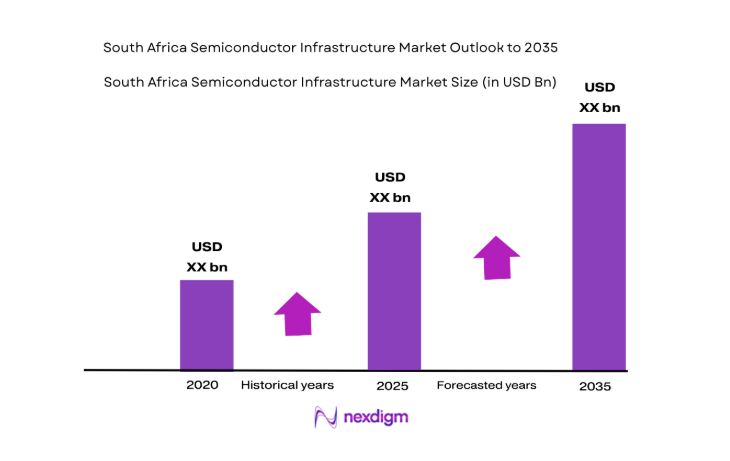
South Africa’s semiconductor infrastructure market is valued at approximately USD ~ billion based on a recent historical assessment, supported by capital investments in microelectronics fabrication pilots, packaging facilities, and advanced electronics manufacturing zones reported by national industrial agencies and international semiconductor equipment trade data. Growth is driven by demand for automotive power electronics, renewable energy semiconductors, and localized chip testing capacity, alongside public funding programs targeting domestic electronics value chain development and supply security.
The market is concentrated in Gauteng, Western Cape, and KwaZulu-Natal, where advanced manufacturing clusters, research universities, and electronics industrial parks provide cleanroom infrastructure, skilled engineering talent, and logistics connectivity to ports and automotive hubs. Pretoria and Johannesburg host defense and aerospace electronics programs, while Cape Town’s microelectronics research ecosystem and Durban’s port-linked manufacturing zones support semiconductor assembly and testing activities through integrated supply chains and export-oriented industrial policy.
Market Segmentation
By Product Type
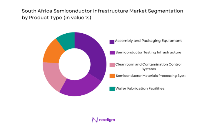
South Africa Semiconductor Infrastructure Market is segmented by product type into wafer fabrication facilities, semiconductor assembly and packaging equipment, semiconductor testing infrastructure, cleanroom and fab support systems, and semiconductor materials processing systems. Recently, semiconductor assembly and packaging equipment has a dominant market share due to factors such as demand patterns, brand presence, infrastructure availability, and consumer preference, particularly reflecting the country’s strategic positioning as a regional hub for electronics assembly, automotive electronics packaging, and export-oriented semiconductor back-end processing aligned with existing manufacturing ecosystems and moderate capital requirements compared with full-scale wafer fabrication plants.
By Platform Type
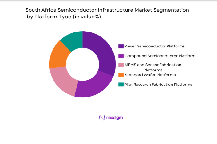
South Africa Semiconductor Infrastructure Market is segmented by platform type into standard wafer platforms, compound semiconductor platforms, MEMS and sensor fabrication platforms, power semiconductor platforms, and pilot research fabrication platforms. Recently, power semiconductor platforms has a dominant market share due to factors such as demand patterns, brand presence, infrastructure availability, and consumer preference, reflecting strong regional demand for power management chips in renewable energy systems, electric mobility components, and industrial automation electronics, alongside national initiatives encouraging localized production of energy-efficient semiconductor devices suitable for African grid and electrification conditions.
Competitive Landscape
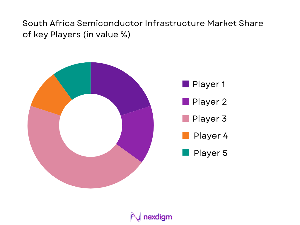
The South Africa semiconductor infrastructure market exhibits moderate consolidation with global semiconductor equipment suppliers collaborating with local electronics and defense manufacturers, while domestic firms focus on specialized assembly, testing, and materials processing niches. Market influence is shaped by multinational lithography and fabrication technology providers, integrated device manufacturers investing in regional packaging lines, and state-supported microelectronics initiatives fostering partnerships between international technology leaders and South African industrial clusters.
| Company Name | Establishment Year | Headquarters | Technology Focus | Market Reach | Key Products | Revenue | Local Infrastructure Presence |
| ASML Holding | 1984 | Netherlands | ~ | ~ | ~ | ~ | ~ |
| Applied Materials | 1967 | USA | ~ | ~ | ~ | ~ | ~ |
| Lam Research | 1980 | USA | ~ | ~ | ~ | ~ | ~ |
| STMicroelectronics | 1987 | Switzerland | ~ | ~ | ~ | ~ | ~ |
| Reutech Radar Systems | 1987 | South Africa | ~ | ~ | ~ | ~ | ~ |
South Africa Semiconductor Infrastructure Market Analysis
Growth Drivers
Localization of semiconductor back-end manufacturing and packaging capacity
The accelerating in South Africa as electronics manufacturers and automotive component producers seek regional supply chain resilience and reduced import dependency for semiconductor components critical to energy systems, mobility electronics, and industrial automation equipment across the African continent. Public industrial policy programs promoting domestic electronics value chain development are supporting investments in semiconductor assembly, testing, and packaging infrastructure, enabling companies to establish facilities aligned with existing manufacturing clusters and export logistics corridors. Automotive electrification trends are expanding demand for power modules, sensors, and control chips assembled locally to meet regional vehicle production requirements and after-sales service markets. Renewable energy deployment across Africa is driving demand for power semiconductor packaging and testing capabilities to support inverters, grid equipment, and energy storage electronics assembled within South African industrial zones. Moderate capital intensity relative to front-end wafer fabrication enables domestic firms and international partners to invest in packaging lines, cleanrooms, and testing systems with faster deployment timelines and lower financial risk compared with full fabrication plants. Government incentives and trade frameworks are encouraging localization of electronic component manufacturing to strengthen supply security for strategic sectors such as defense, energy, and transportation. Industrial parks in Gauteng and KwaZulu-Natal provide utilities, logistics access, and skilled labor pools that support semiconductor back-end operations integrated with electronics assembly ecosystems. Increasing regional electronics consumption in telecommunications, consumer devices, and industrial automation is creating sustained demand for locally packaged semiconductor components tailored to African environmental and reliability requirements.
Expansion of compound and power semiconductor applications in energy and mobility sectors
The sectors is strengthening demand for specialized semiconductor infrastructure in South Africa as renewable energy systems, electric mobility components, and industrial power electronics adoption increases across national and regional markets. Power management and conversion devices based on silicon carbide and gallium nitride technologies are essential for solar inverters, battery systems, and electric drivetrain electronics deployed in African electrification and transportation initiatives. Domestic manufacturing strategies emphasize localized production and testing of robust power semiconductors capable of operating in high-temperature and variable-grid conditions common in emerging energy networks. Automotive manufacturing activity in South Africa is transitioning toward electrified and hybrid vehicle platforms requiring advanced power modules and control electronics assembled and qualified locally. Defense and aerospace electronics programs also demand radiation-tolerant and high-reliability compound semiconductor devices for radar, communication, and sensing systems developed within national security supply chains. Research institutions and microelectronics laboratories in Cape Town and Pretoria are expanding compound semiconductor pilot lines and materials processing capabilities supporting industrial technology transfer. Global semiconductor firms are partnering with regional manufacturers to establish packaging and testing capabilities tailored to power and RF semiconductor products serving African markets. Growth in industrial automation, telecommunications infrastructure, and smart grid equipment further reinforces demand for compound semiconductor devices produced or assembled within South Africa.
Market Challenges
High capital and infrastructure requirements for semiconductor fabrication ecosystems
limit the development of advanced semiconductor infrastructure in South Africa because establishing wafer fabrication facilities demands substantial investment in ultra-clean environments, precision equipment, and continuous utilities that exceed the financial capacity of many domestic industrial stakeholders. Semiconductor fabs require stable high-capacity electricity, ultra-pure water supply, and specialized chemical handling systems, creating infrastructure burdens in regions where energy reliability and water management remain national challenges. Equipment procurement costs for lithography, deposition, and etch systems are dominated by global suppliers, exposing projects to currency volatility and import dependency risks that elevate investment uncertainty. Limited local supply chains for semiconductor materials and process chemicals further increase operating costs and logistical complexity for potential fabrication facilities. Skilled workforce requirements in microelectronics process engineering and equipment maintenance exceed the current availability of trained semiconductor specialists in the domestic labor market. Financial institutions and investors perceive semiconductor fabrication projects as high risk due to long payback periods and technological obsolescence cycles, constraining access to capital. National industrial policies prioritize downstream electronics manufacturing and packaging activities rather than front-end wafer fabrication because of these structural constraints. Consequently, the market remains focused on assembly, testing, and niche semiconductor infrastructure segments rather than full fabrication ecosystem development.
Dependence on imported semiconductor equipment, materials, and technology expertise
Constrains the scalability and competitiveness of South Africa’s semiconductor infrastructure because nearly all advanced fabrication, packaging, and testing technologies originate from global suppliers located in Europe, Asia, and North America. Import reliance increases procurement lead times and exposes infrastructure projects to international trade controls and export regulations affecting semiconductor manufacturing equipment. Limited domestic production of semiconductor wafers, specialty gases, and advanced packaging materials forces manufacturers to maintain complex international supply chains vulnerable to geopolitical disruptions. Technology transfer agreements with multinational firms often involve intellectual property restrictions that limit local process innovation and independent capability development. Maintenance and calibration of semiconductor equipment require foreign technical support and spare parts, increasing operational costs and downtime risks. Currency fluctuations influence the affordability of imported semiconductor systems and materials, complicating investment planning for domestic firms. Skills gaps in advanced semiconductor process engineering necessitate foreign training programs and expatriate expertise, slowing the development of self-sustaining industrial capabilities. These dependencies collectively restrict the country’s ability to expand semiconductor infrastructure beyond assembly and testing segments into higher-value manufacturing domains.
Opportunities
Development of regional semiconductor packaging and testing hub serving African electronics markets
Represents a significant opportunity for South Africa as the continent’s electronics consumption expands in telecommunications, renewable energy, mobility, and industrial automation sectors requiring reliable semiconductor components. South Africa’s established manufacturing zones, logistics connectivity, and technical workforce position the country to provide back-end semiconductor services to neighboring economies lacking advanced electronics infrastructure. Automotive production clusters and export corridors enable integration of semiconductor packaging operations with vehicle electronics supply chains serving regional assembly plants. Renewable energy deployment across Africa creates demand for locally packaged power modules and control chips designed for environmental durability and grid variability conditions. Government industrialization strategies promoting high-tech manufacturing localization support investment incentives for semiconductor assembly and testing facilities targeting continental markets. Partnerships with global semiconductor firms can transfer packaging technologies and quality standards to domestic facilities serving Africa-specific device requirements. Expansion of telecommunications infrastructure and consumer electronics adoption across African countries generates sustained semiconductor demand addressable through regional packaging hubs. Establishing South Africa as a semiconductor back-end center strengthens supply chain resilience and reduces import dependency for multiple African industries.
Expansion of compound semiconductor research and pilot fabrication for niche high-reliability applications
offers strategic growth potential for South Africa due to existing microelectronics research institutions and defense technology programs focused on advanced sensing, communication, and power electronics devices. Compound semiconductor technologies such as gallium nitride and silicon carbide enable high-efficiency and high-temperature performance suitable for renewable energy systems, aerospace electronics, and telecommunications infrastructure prevalent in African markets. Research laboratories and pilot fabrication lines can develop specialized devices tailored to regional environmental conditions and industrial requirements rather than competing in mass-market logic semiconductor production. Collaboration between universities, defense agencies, and industrial manufacturers can accelerate technology transfer from research prototypes to commercial niche products. Export opportunities exist for high-reliability semiconductor components used in satellite communication, radar sensing, and harsh-environment energy systems deployed across emerging economies. Government funding programs supporting microelectronics innovation and advanced materials research can strengthen compound semiconductor capabilities within national technology strategies. Partnerships with international compound semiconductor firms may establish localized pilot production and packaging capabilities aligned with regional demand. Such specialization allows South Africa to participate in high-value semiconductor segments without requiring large-scale silicon wafer fabrication infrastructure.
Future Outlook
South Africa’s semiconductor infrastructure market is expected to expand steadily over the next five years as regional electronics demand, renewable energy deployment, and automotive electrification increase requirements for locally assembled and tested semiconductor devices. Technological progress in compound and power semiconductor applications will encourage pilot fabrication and packaging investments. Government industrial localization strategies and export-oriented manufacturing policies are likely to strengthen infrastructure development. Partnerships with global semiconductor firms and regional supply chain integration will further support sustainable market growth.
Major Players
- ASML Holding
- Applied Materials
- Lam Research
- Tokyo Electron
- KLA Corporation
- ASM International
- SCREEN Semiconductor Solutions
- TSMC
- Samsung Electronics
- Intel Corporation
- GlobalFoundries
- STMicroelectronics
- TeracoData Environments
- ReutechRadar Systems
- SUSSMicroTec
Key Target Audience
- Semiconductor device manufacturers
- Electronics manufacturing companies
- Automotivecomponentmanufacturers
- Renewable energy equipment producers
- Defense and aerospace organizations
- Investments and venture capitalist firms
- Government and regulatory bodies
- Industrial automation companies
Research Methodology
Step 1: Identification of Key Variables
Key market variables including semiconductor infrastructure types, investment flows, manufacturing capacity indicators, and regional electronics demand drivers were identified through industrial policy documents, semiconductor trade statistics, and technology adoption trends. Supply chain components such as materials, equipment, and fabrication processes were mapped to define market boundaries.
Step 2: Market Analysis and Construction
Market structure was constructed by integrating infrastructure investment data, equipment deployment patterns, and manufacturing cluster analysis across South African regions. Segmentation models categorized infrastructure by product and platform type, aligning with semiconductor value chain stages and regional industrial ecosystems.
Step 3: Hypothesis Validation and Expert Consultation
Preliminary findings were validated through consultations with semiconductor engineers, electronics manufacturers, and industrial policy specialists familiar with South African microelectronics initiatives. Cross-verification with international semiconductor equipment deployment trends ensured consistency with global industry dynamics.
Step 4: Research Synthesis and Final Output
Validated datasets and qualitative insights were synthesized into a comprehensive market framework covering segmentation, competitive landscape, and growth factors. Analytical outputs were structured to reflect investment trends, technological evolution, and regional industrial capabilities influencing semiconductor infrastructure development.
- Executive Summary
- Research Methodology (Definitions, Scope, Industry Assumptions, Market Sizing Approach, Primary & Secondary Research Framework, Data Collection & Verification Protocol, Analytic Models & Forecast Methodology, Limitations & Research Validity Checks)
- Market Definition and Scope
- Value Chain & Stakeholder Ecosystem
- Regulatory / Certification Landscape
- Sector Dynamics Affecting Demand
- Strategic Initiatives & Infrastructure Growth

- Growth Drivers
Government initiatives to localize semiconductor manufacturing capacity
Rising demand for automotive and power electronics chips in Africa
Expansion of electronics assembly and testing ecosystems
Strategic investments in research fabs and microelectronics labs
Growing adoption of compound semiconductor technologies - Market Challenges
High capital intensity of semiconductor fabrication facilities
Limited domestic semiconductor manufacturing expertise
Dependence on imported semiconductor equipment and materials
Infrastructure constraints in power and ultra-pure water supply
Small local demand base for advanced logic semiconductors - Market Opportunities
Development of compound semiconductor fabs for power and RF devices
Regional semiconductor packaging and testing hub potential
Public-private partnerships in semiconductor research infrastructure - Trends
Shift toward specialized and niche semiconductor fabrication lines
Integration of semiconductor R&D facilities with universities
Adoption of modular and pilot semiconductor fabs
Growth in power electronics and sensor chip production
Increasing collaboration with global semiconductor equipment vendors - Government Regulations & Defense Policy
National strategies promoting electronics and semiconductor localization
Incentives for high-tech manufacturing infrastructure investment
Export and technology transfer controls affecting semiconductor equipment - SWOT Analysis
- Stakeholder and Ecosystem Analysis
- Porter’s Five Forces Analysis
- Competition Intensity and Ecosystem Mapping
- By Market Value, 2020-2025
- By Installed Units, 2020-2025
- By Average System Price, 2020-2025
- By System Complexity Tier, 2020-2025
- By System Type (In Value%)
Wafer Fabrication Facilities
Semiconductor Assembly and Packaging Lines
Semiconductor Testing Infrastructure
Cleanroom and Fab Support Systems
Semiconductor Materials Processing Systems - By Platform Type (In Value%)
300mm Wafer Production Platforms
200mm Wafer Production Platforms
Compound Semiconductor Platforms
MEMS and Sensor Fabrication Platforms
Power and Analog Semiconductor Platforms - By Fitment Type (In Value%)
Greenfield Semiconductor Fabs
Brownfield Fab Expansions
Modular Fab Units
Research and Pilot Line Facilities
Specialized Semiconductor Labs - By End User Segment (In Value%)
Integrated Device Manufacturers
Foundry Service Providers
Research Institutes and Universities
Electronics Manufacturing Firms
Defense and Aerospace Electronics Units - By Procurement Channel (In Value%)
Direct OEM Procurement
EPC and Turnkey Contractors
Government Semiconductor Programs
Technology Partnerships and Joint Ventures
Refurbished Equipment Suppliers - By Material / Technology (in Value %)
Silicon Wafer Processing Technology
Compound Semiconductor Materials
Advanced Lithography Technology
Thin Film Deposition and Etch Technology
Semiconductor Packaging Materials
- Market structure and competitive positioning
Market share snapshot of major players - Cross Comparison Parameters (Technology Node Capability, Wafer Size Support, Fab Automation Level, Process Technology Portfolio, Local Service Presence, Installation Base, End User Focus, Partnership Ecosystem, Infrastructure Integration Capability)
- SWOT Analysis of Key Competitors
- Pricing & Procurement Analysis
- Key Players
ASML Holding
Applied Materials
Lam Research
Tokyo Electron
KLA Corporation
ASM International
SCREEN Semiconductor Solutions
TSMC
Samsung Electronics
Intel Corporation
GlobalFoundries
STMicroelectronics
Teraco Data Environments
Reutech Radar Systems
SUSS MicroTec
- Integrated device manufacturers seeking localized fabrication and packaging capacity
- Research institutions expanding semiconductor pilot line capabilities
- Electronics manufacturers demanding regional testing and packaging services
- Defense and aerospace sector requiring secure semiconductor supply chains
- Forecast Market Value, 2026-2035
- Forecast Installed Units, 2026-2035
- Price Forecast by System Tier, 2026-2035
- Future Demand by Platform, 2026-2035


 Request a Sample
 Ask for Customization
 Get a Quote
 Enquire Now