
 Download PDF
 Download PDF
Market Overview
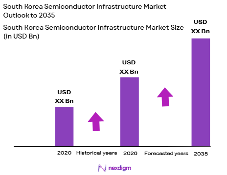
South Korea semiconductor infrastructure market is valued at approximately USD ~ billion based on a recent historical assessment, driven by large-scale fab expansions, advanced packaging capacity growth, and national semiconductor competitiveness initiatives. Capital investments by memory leaders and foundry operators sustain demand for wafer fabrication equipment, cleanroom systems, and utility infrastructure. Expansion of high-bandwidth memory and advanced node production further accelerates facility upgrades, automation systems, and materials handling infrastructure across the domestic semiconductor manufacturing ecosystem.
Gyeonggi Province dominates the South Korea semiconductor infrastructure market due to concentration of memory fabs, equipment suppliers, and advanced packaging clusters around Suwon, Icheon, and Pyeongtaek. Chungcheong regions host major fabrication complexes and materials suppliers benefiting from industrial land availability and logistics connectivity. Seoul anchors design and R&D infrastructure supporting semiconductor innovation. Proximity between fabs, equipment vendors, and research institutes enables integrated supply chains and rapid technology deployment across the national semiconductor production network.
Market Segmentation
By Infrastructure Type
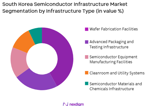
South Korea Semiconductor Infrastructure market is segmented by product type into wafer fabrication facilities, advanced packaging and testing infrastructure, semiconductor materials and chemicals infrastructure, semiconductor equipment manufacturing facilities, and cleanroom and utility systems. Recently, wafer fabrication facilities have a dominant market share due to factors such as sustained memory production expansion, advanced node migration, government fab incentives, and strong domestic chip demand. Large-scale investments in new memory fabs and foundry capacity require extensive infrastructure including lithography halls, process tool bays, and automation corridors. National semiconductor strategy prioritizes fabrication capacity leadership, reinforcing capital allocation toward fab construction and upgrades. Continuous node shrink and yield optimization programs require facility retrofits and expansion. Concentration of global memory leaders in South Korea further amplifies fab infrastructure spending compared with other semiconductor infrastructure segments.
By End-Use Application
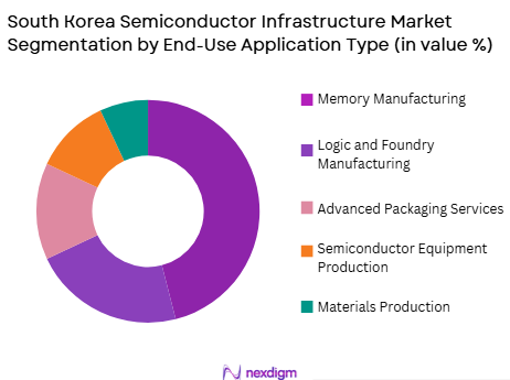
South Korea Semiconductor Infrastructure market is segmented by end-use application into memory manufacturing, logic and foundry manufacturing, advanced packaging services, semiconductor equipment production, and materials production. Recently, memory manufacturing has a dominant market share due to factors such as global leadership of domestic DRAM and NAND producers, ongoing high-bandwidth memory scaling, and sustained fab expansion programs. Memory producers continuously upgrade and expand facilities to maintain technology leadership and production volume. Integration of advanced packaging for stacked memory further increases infrastructure needs. Strong export orientation of memory chips drives capacity investment cycles. Government support for strategic memory technology reinforces capital expenditure concentration in memory manufacturing infrastructure relative to other semiconductor applications in South Korea.
Competitive Landscape
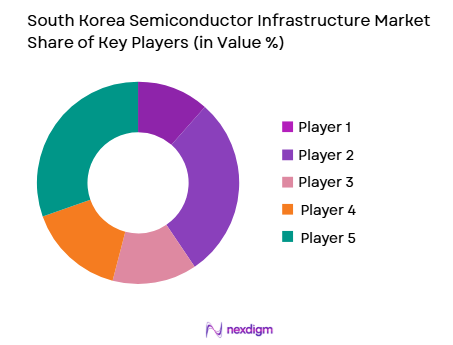
The South Korea semiconductor infrastructure market is highly consolidated around major memory manufacturers and a network of specialized construction, equipment, and materials firms supporting fab development. Large conglomerates drive capital expenditure cycles that shape supplier ecosystems. Global semiconductor equipment vendors collaborate with domestic engineering and facility companies. Strategic partnerships between chipmakers and infrastructure contractors determine project scale and technology adoption across fabrication and packaging facilities.
| Company Name | Establishment Year | Headquarters | Technology Focus | Market Reach | Key Products | Revenue | Fab Construction Expertise |
| Samsung Electronics | 1969 | Suwon, South Korea | ~ | ~ | ~ | ~ | ~ |
| SK hynix | 1983 | Icheon, South Korea | ~ | ~ | ~ | ~ | ~ |
| Samsung Engineering | 1970 | Seoul, South Korea | ~ | ~ | ~ | ~ | ~ |
| Tokyo Electron | 1963 | Tokyo, Japan | ~ | ~ | ~ | ~ | ~ |
| ASML | 1984 | Veldhoven, Netherlands | ~ | ~ | ~ | ~ | ~ |
South Korea Semiconductor Infrastructure Market Analysis
Growth Drivers
National Semiconductor Capacity Expansion and Strategic Fab Investments
South Korea’s position as a global semiconductor leader is reinforced by continuous expansion of wafer fabrication capacity supported by coordinated corporate and government investment programs. Memory manufacturers are constructing new megafabs and upgrading existing facilities to maintain technology leadership in advanced DRAM, NAND, and high-bandwidth memory production. Foundry capacity expansion supports domestic logic chip demand and diversification beyond memory. National semiconductor strategies provide tax incentives, infrastructure funding, and land development support for fab construction. Large-scale fabrication projects require extensive cleanroom, utilities, automation, and materials handling infrastructure. Equipment installation cycles stimulate facility upgrades and retrofits. Supply chain localization initiatives expand domestic materials and component manufacturing infrastructure. Regional semiconductor clusters enable shared utilities and logistics systems. Continuous technology node transitions necessitate facility modernization. These structural investment dynamics sustain long-term growth of semiconductor infrastructure across fabrication ecosystems.
Advanced Packaging, Heterogeneous Integration, and HBM Manufacturing Expansion
Rapid growth of advanced packaging technologies and high-bandwidth memory manufacturing is transforming semiconductor infrastructure requirements in South Korea. Stacked memory and heterogeneous integration demand specialized packaging facilities with precision bonding, through-silicon-via processing, and thermal management capabilities. Memory leaders are expanding advanced packaging capacity to support AI chip demand. Integration of packaging within fabrication complexes increases infrastructure scale and complexity. Equipment for wafer-level packaging and 3D stacking requires dedicated cleanroom environments. Supply chain expansion includes substrates, interposers, and advanced materials infrastructure. Packaging process integration shortens production cycles and improves performance. Domestic development of advanced packaging strengthens competitiveness in AI semiconductor markets. Investments in co-packaged optics and chiplet assembly further expand infrastructure scope. These technology shifts drive sustained capital expenditure in packaging and integration facilities nationwide.
Market Challenges
High Capital Intensity and Cyclical Semiconductor Investment Patterns
Semiconductor infrastructure development in South Korea requires extremely high capital expenditure and is closely tied to cyclical demand patterns in global semiconductor markets. Memory price fluctuations influence fab investment timing and scale. Periods of oversupply can delay infrastructure projects and reduce equipment utilization. Large upfront costs for fab construction, utilities, and cleanroom systems create financial risk. Infrastructure suppliers depend on concentrated customer base of major chipmakers. Project delays or cancellations can disrupt supply chains. Financing large fabrication complexes requires long-term demand visibility. Cyclical downturns affect contractor capacity utilization. Maintaining readiness for next investment cycle increases fixed costs. These cyclical dynamics create volatility in semiconductor infrastructure demand and planning.
Land, Power, and Environmental Constraints on Fab Expansion
Expansion of semiconductor fabrication infrastructure in South Korea faces constraints related to industrial land availability, power supply capacity, and environmental regulations. Megafab facilities require large contiguous sites with access to water and electricity. Urban density limits suitable locations near existing clusters. Power demand of advanced fabs strains regional grids. Water consumption and waste management requirements impose environmental compliance costs. Community concerns about industrial expansion can delay approvals. Infrastructure for utilities and logistics must scale with fab size. Energy sustainability targets influence facility design and operation. Regulatory processes extend project timelines. These constraints complicate rapid scaling of semiconductor infrastructure nationwide.
Opportunities
Localization of Semiconductor Materials and Equipment Manufacturing Ecosystem
South Korea has opportunity to expand domestic production of semiconductor materials and equipment to strengthen infrastructure self-sufficiency and reduce import dependence. Government semiconductor initiatives support local suppliers of photoresists, gases, substrates, and process tools. Co-location of materials and equipment manufacturing near fabs improves supply reliability. Domestic equipment innovation can address specialized memory and packaging processes. Supply chain localization enhances resilience against trade disruptions. Infrastructure expansion for materials plants and tool manufacturing facilities increases industrial capacity. Collaboration between chipmakers and local suppliers accelerates technology transfer. Export potential exists for regionally competitive semiconductor equipment. Strengthened domestic ecosystem supports long-term infrastructure growth. Localization initiatives align with national semiconductor competitiveness strategy.
Global Foundry Diversification and International Fab Collaboration
South Korea can leverage its semiconductor expertise to participate in international fab construction and infrastructure projects as global chipmakers diversify manufacturing locations. Korean engineering and construction firms possess advanced fab development capabilities. Partnerships with overseas semiconductor investors enable export of infrastructure services. Participation in global semiconductor supply chains expands revenue streams beyond domestic investment cycles. International collaboration in advanced packaging and materials facilities increases global presence. Technology transfer and joint ventures support market entry in emerging semiconductor regions. Korean firms can provide turnkey fab infrastructure solutions. Overseas projects mitigate domestic cyclicality risks. This opportunity positions South Korea as a global semiconductor infrastructure provider.
Future Outlook
South Korea semiconductor infrastructure market is expected to expand steadily as advanced memory scaling, packaging integration, and fab modernization programs continue across major semiconductor clusters. Government semiconductor strategies will support facility expansion and supply chain localization. Advanced node transitions and AI-driven chip demand will require new fabrication and packaging infrastructure. Sustainability and energy efficiency requirements will shape future fab design and utilities systems nationwide.
Major Players
- Samsung Electronics
- SK hynix
- Samsung Engineering
- Tokyo Electron
- ASML
- Applied Materials
- Lam Research
- KLA
- Wonik IPS
- SEMES
- Jusung Engineering
- PSK Holdings
- KC Tech
- Daeduck Electronics
- Hanmi Semiconductor
Key Targets
- Semiconductor manufacturers
- Semiconductor equipment suppliers
- Materials and chemicals producers
- Fab construction contractors
- Advanced packaging firms
- Investments and venture capitalist firms
- Government and regulatory bodies
- Industrial infrastructure developers
Research Methodology
Step 1: Identification of Key Variables
Key variables include fab capacity additions, semiconductor capital expenditure, packaging facility investments, equipment deployment cycles, and materials production capacity. Variables are mapped across infrastructure segments and regional clusters to define market structure.
Step 2: Market Analysis and Construction
Supply-side analysis evaluates fabrication, packaging, and equipment infrastructure expansion, while demand-side analysis examines semiconductor production and technology transitions. Data triangulation constructs market size and segmentation estimates.
Step 3: Hypothesis Validation and Expert Consultation
Industry experts from semiconductor manufacturers, equipment suppliers, and engineering firms validate assumptions on infrastructure growth, technology adoption, and investment cycles. Feedback refines segmentation shares and competitive positioning.
Step 4: Research Synthesis and Final Output
Validated quantitative datasets and qualitative insights are synthesized into infrastructure forecasts, competitive analysis, and strategic outlook. Consistency checks ensure alignment across market size, segmentation, and technology narratives.
- Executive Summary
- Research Methodology (Definitions, Scope, Industry Assumptions, Market Sizing Approach, Primary & Secondary Research Framework, Data Collection & Verification Protocol, Analytic Models & Forecast Methodology, Limitations & Research Validity Checks)
- Market Definition and Scope
- Value Chain & Stakeholder Ecosystem
- Regulatory / Certification Landscape
- Sector Dynamics Affecting Demand
- Strategic Initiatives & Infrastructure Growth

- Growth Drivers
Global leadership in memory and advanced semiconductor production
Strong national investment in semiconductor fabs and clusters
Rising demand for advanced packaging and heterogeneous integration - Market Challenges
Extremely high capital and energy requirements of advanced fabs
Dependence on foreign lithography and specialty equipment
Environmental and regulatory constraints on fab expansion - Market Opportunities
Next-generation semiconductor fabs and advanced nodes
Advanced packaging and chiplet integration facilities
Localization of semiconductor materials and equipment supply - Trends
Transition to sub-5nm and gate-all-around process nodes
Expansion of advanced packaging and 3D integration lines
Smart fab automation and digital twin manufacturing systems - Government regulations
National semiconductor industry promotion policies
Export control and technology security regulations
Environmental and energy compliance for fabs - SWOT analysis
- Porters five forces
- By Market Value, 2020-2025
- By Installed Units, 2020-2025
- By Average System Price, 2020-2025
- By System Complexity Tier, 2020-2025
- By System Type (In Value%)
Wafer Fabrication Facilities
Advanced Packaging Lines
Semiconductor Test and Inspection Systems
Cleanroom and Fab Support Infrastructure
Semiconductor Materials Handling Systems - By Platform Type (In Value%)
Integrated Device Manufacturer Fabs
Foundry Facilities
OSAT Facilities
Research and Pilot Production Labs
Semiconductor Industrial Clusters - By Fitment Type (In Value%)
Greenfield Fab Construction
Brownfield Fab Expansion
Equipment Retrofit and Upgrade
Modular Production Line Integration
Automation and Robotics Integration - By EndUser Segment (In Value%)
Memory and Logic IDMs
Foundry Operators
OSAT Providers
Equipment and Materials Suppliers
Government and Research Institutes - By Procurement Channel (In Value%)
Direct Equipment Procurement
EPC and Turnkey Contracts
OEM Integrated Supply
Distributor and Agent Supply
Government Incentive Programs
- Market Share Analysis
- Cross Comparison Parameters (Process Node Capability, Lithography Technology Compatibility, Packaging Technology Capability, Production Automation Level, Cleanroom Class Standard, Yield Optimization Systems, Capacity Scalability, Materials Handling Automation, Test and Metrology Integration, Energy and Utility Efficiency, Facility Expansion Flexibility, Supply Chain Localization Level)
- SWOT Analysis of Key Competitors
- Pricing & Procurement Analysis
- Key Players
Samsung Electronics
SK hynix
DB HiTek
Magnachip Semiconductor
LX Semicon
Amkor Technology Korea
ASE Korea
Hanmi Semiconductor
Wonik IPS
SEMES
PSK Group
Eugene Technology
Jusung Engineering
SFA Engineering
TES Co
- Forecast Market Value, 2026-2035
- Forecast Installed Units, 2026-2035
- Price Forecast by System Tier, 2026-2035
- Future Demand by Platform, 2026-2035


 Request a Sample
 Ask for Customization
 Get a Quote
 Enquire Now