
 Download PDF
Market Overview
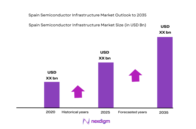
Spain’s semiconductor infrastructure market reached approximately USD ~ billion in total capital and facility investment value based on a recent historical assessment, driven by European Chips Act funding allocations, national semiconductor strategy incentives, and automotive electronics localization programs. Infrastructure demand is expanding across wafer fabrication utilities, advanced packaging lines, and cleanroom construction as Spain positions itself within the European microelectronics manufacturing ecosystem through public-private fab initiatives and industrial cluster development.
Barcelona, Madrid, and Valencia dominate Spain’s semiconductor infrastructure activity due to established electronics manufacturing bases, research microelectronics institutes, and proximity to automotive and aerospace supply chains. Barcelona hosts major photonics and compound semiconductor research facilities, Madrid concentrates national semiconductor policy institutions and engineering firms, while Valencia benefits from industrial land availability and port logistics connectivity supporting fab construction and semiconductor equipment import operations.
Market Segmentation
By Product Type
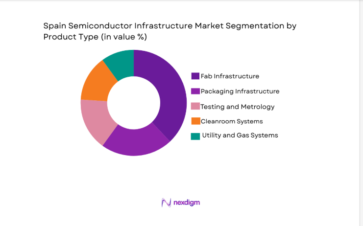
Spain Semiconductor Infrastructure market is segmented by product type into wafer fabrication facility infrastructure, assembly and packaging infrastructure, semiconductor testing and metrology infrastructure, cleanroom and contamination control systems, and semiconductor utility and gas delivery systems. Fab infrastructure dominates due to highest capital intensity, complex utility integration, and policy-driven wafer fabrication facility investments within Spain’s semiconductor manufacturing strategy.
By Platform Type
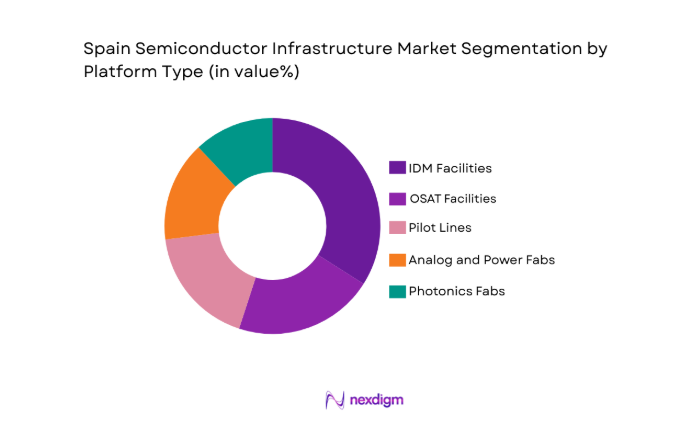
Spain Semiconductor Infrastructure market is segmented by platform type into integrated device manufacturer facilities, outsourced semiconductor assembly and test facilities, research and pilot fabrication lines, specialty analog and power semiconductor fabs, and photonics and compound semiconductor facilities. Integrated device manufacturer facilities dominate due to national semiconductor manufacturing localization, automotive semiconductor demand, and large integrated fab campus investments within Spain.
Competitive Landscape
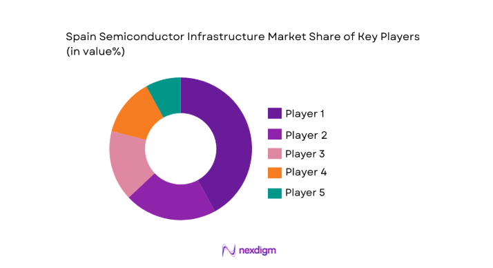
Spain semiconductor infrastructure market exhibits moderate consolidation, with European engineering-procurement-construction firms and global semiconductor facility specialists dominating large fab projects, while domestic industrial engineering companies support utilities, cleanrooms, and facility integration. Major players leverage experience in semiconductor plant construction, process utilities, and EU-funded infrastructure programs to secure projects, resulting in collaborative consortia structures combining international technology expertise with local regulatory and construction capabilities.
| Company Name | Establishment Year | Headquarters | Technology Focus | Market Reach | Key Products | Revenue | Fab Projects in Spain |
| Exyte | 1912 | Germany | ~ | ~
|
~ | ~ | ~ |
| Ferrovial | 1952 | Spain | ~ | ~ | ~ | ~ | ~ |
| Acciona Industrial | 1997 | Spain | ~ | ~ | ~ | ~ | ~ |
| Air Liquide Engineering & Construction | 1962 | France | ~ | ~ | ~ | ~ | ~ |
| Fluor Corporation | 1912 | USA | ~ | ~ | ~ | ~ | ~ |
Spain Semiconductor Infrastructure Market Analysis
Growth Drivers
European Semiconductor Sovereignty Investment Programs
Spain semiconductor infrastructure expansion is strongly propelled by coordinated European semiconductor sovereignty programs that allocate multi-billion-dollar funding toward domestic chip manufacturing capacity, research fabs, and advanced packaging facilities across member states, with Spain positioned as a strategic southern European manufacturing hub within this framework. These programs incentivize construction of wafer fabrication plants, cleanrooms, and semiconductor utilities through subsidies, tax incentives, and public-private partnerships that significantly reduce investment risk for infrastructure developers and semiconductor firms entering Spain. National semiconductor strategies complement European initiatives by targeting automotive electronics, power semiconductors, and photonics manufacturing clusters, which require large-scale facility development and associated infrastructure engineering services. Infrastructure demand is amplified because semiconductor fabs represent some of the most capital-intensive industrial facilities globally, requiring extensive power, water, chemical handling, and contamination control systems that multiply engineering and construction spending per manufacturing site. Spain benefits from geographic proximity to European automotive manufacturing corridors and renewable energy resources, enabling policymakers to justify infrastructure investment as part of resilient supply chain strategy, thereby accelerating approvals and funding flows. Semiconductor infrastructure projects also create high-skilled employment and regional industrial development, aligning with economic policy priorities that further reinforce political support and financing availability. European funding mechanisms require domestic facility development rather than offshore manufacturing reliance, ensuring sustained infrastructure investment pipelines within Spain. Consequently, semiconductor infrastructure firms experience long-term project visibility and capacity utilization growth driven by policy-anchored demand rather than purely cyclical semiconductor market fluctuations.
Automotive and Power Electronics Manufacturing Localization
Spain’s position as a major European automotive manufacturing base creates substantial demand for localized semiconductor production infrastructure, particularly for power electronics, sensors, and automotive-grade integrated circuits that support electrification and advanced driver systems, thereby stimulating fab and packaging facility development within the country. Automotive manufacturers increasingly seek geographically proximate semiconductor supply to mitigate supply disruptions experienced in recent industry shortages, which encourages joint ventures and supplier facilities near vehicle production clusters. Power semiconductor fabrication requires specialized cleanroom, wafer processing, and packaging infrastructure distinct from consumer electronics chips, resulting in targeted infrastructure investment programs within Spain’s industrial regions. Electrification trends in vehicles expand semiconductor content per vehicle, increasing long-term demand visibility that justifies capital expenditure in domestic semiconductor manufacturing facilities and associated utilities infrastructure. Spain’s renewable energy capacity supports energy-intensive semiconductor plants with lower carbon intensity electricity, aligning with sustainability requirements of automotive and electronics firms and making local infrastructure development more attractive than external sourcing. Regional governments promote semiconductor manufacturing near automotive hubs through land incentives and industrial park development, concentrating infrastructure spending geographically and accelerating project execution timelines. Collaboration between automotive OEMs and semiconductor firms drives integrated manufacturing campuses combining wafer fabrication and advanced packaging, further increasing infrastructure complexity and investment scale. These factors collectively create sustained infrastructure demand anchored in industrial manufacturing localization rather than purely research-driven semiconductor initiatives.
Market Challenges
Dependence on Imported Semiconductor Equipment and Technology
Spain semiconductor infrastructure development faces structural constraints due to reliance on imported advanced semiconductor equipment, process technologies, and facility design expertise from established semiconductor manufacturing nations, which increases project costs, extends timelines, and limits domestic value capture within infrastructure investments. Semiconductor fabrication plants require highly specialized lithography, deposition, and metrology equipment supplied by a small number of global vendors, and infrastructure must be designed around these technologies, reducing flexibility for local engineering firms lacking proprietary semiconductor process knowledge. Import dependence also exposes infrastructure projects to geopolitical export controls and supply chain disruptions affecting equipment availability, thereby creating uncertainty in facility commissioning schedules. Domestic semiconductor ecosystem maturity remains limited compared with leading manufacturing countries, resulting in shortages of experienced process engineers, facility designers, and contamination control specialists necessary for complex fab infrastructure implementation. Infrastructure contractors often need to partner with international semiconductor facility experts, which transfers significant project value outside Spain and increases reliance on foreign technical standards and designs. Currency fluctuations and logistics costs associated with importing equipment and specialized materials further increase total infrastructure investment requirements. These dependencies reduce Spain’s ability to rapidly scale semiconductor manufacturing capacity independent of global supply chain dynamics, limiting strategic autonomy objectives underlying national semiconductor policy. Consequently, infrastructure growth is constrained by external technology availability rather than purely domestic demand conditions.
Energy, Water, and Environmental Constraints for Fab Operations
Semiconductor infrastructure projects in Spain encounter significant challenges related to energy supply capacity, ultra-pure water availability, and environmental permitting requirements, as semiconductor fabrication facilities are among the most resource-intensive industrial installations and must comply with stringent environmental regulations governing emissions, water use, and waste management. Large fabs require continuous high-quality electricity supply with minimal interruption, necessitating grid upgrades and dedicated substations that increase infrastructure costs and extend project timelines. Semiconductor processes consume substantial volumes of ultra-pure water for wafer cleaning and chemical processing, and regions with water scarcity concerns face regulatory scrutiny and community opposition to large industrial water usage. Environmental permitting for chemical storage, waste treatment, and emissions control systems is complex and time-consuming, delaying facility construction and commissioning schedules. Public acceptance of large semiconductor plants may be affected by environmental impact perceptions, particularly regarding water and energy consumption, requiring additional mitigation infrastructure and stakeholder engagement efforts. Compliance with European environmental standards increases engineering complexity and capital expenditure for wastewater treatment, air filtration, and hazardous material handling systems integrated into fab infrastructure. Renewable energy integration requirements further complicate power infrastructure design to meet sustainability targets while maintaining process stability. These factors collectively increase cost, regulatory burden, and implementation risk for semiconductor infrastructure expansion within Spain.
Opportunities
Development of Compound Semiconductor and Photonics Manufacturing Clusters
Spain has significant opportunity to expand semiconductor infrastructure through specialization in compound semiconductor and photonics manufacturing clusters, leveraging existing research strengths in optoelectronics and materials science to establish niche fabrication facilities that complement Europe’s broader semiconductor ecosystem while requiring targeted infrastructure investment in specialized processing environments. Compound semiconductor fabrication uses materials such as gallium nitride and indium phosphide that demand distinct cleanroom conditions, chemical handling systems, and epitaxy equipment infrastructure compared with silicon fabs, creating new engineering and construction demand segments within Spain. Photonics devices support telecommunications, sensing, and defense applications with growing European demand, encouraging regional governments to invest in pilot fabs and production facilities that anchor innovation ecosystems. Spain’s universities and research institutes provide technology transfer pipelines that can evolve into commercial manufacturing infrastructure projects when supported by funding and industry partnerships. Specialized semiconductor clusters require smaller but technologically sophisticated facilities, allowing Spain to enter high-value semiconductor markets without competing directly with large-scale silicon manufacturing leaders. European research funding and defense technology programs prioritize photonics and compound semiconductor development, ensuring sustained project pipelines. These clusters can attract global semiconductor firms seeking European manufacturing presence in niche technologies, stimulating foreign direct investment into infrastructure. As compound semiconductor applications expand in power electronics and communication systems, Spain’s focused infrastructure development can secure competitive positioning in emerging semiconductor segments.
Advanced Packaging and Heterogeneous Integration Facilities Expansion
Advanced packaging and heterogeneous integration represent a major opportunity for Spain semiconductor infrastructure growth because these technologies are increasingly critical to semiconductor performance scaling and supply chain resilience, while requiring specialized facility environments that differ from traditional wafer fabrication plants and can be developed with lower capital intensity yet high technological value. Advanced packaging involves wafer-level packaging, chiplet integration, and three-dimensional stacking processes that demand precision assembly cleanrooms, thermal management systems, and metrology infrastructure distinct from front-end fabs. Spain’s semiconductor strategy emphasizes downstream manufacturing and integration capabilities aligned with European electronics industries, creating policy support and funding incentives for packaging infrastructure projects. Packaging facilities can be co-located with automotive electronics manufacturing clusters, strengthening supply chain integration and reducing logistics complexity for semiconductor components used in vehicles and industrial systems. Global semiconductor firms increasingly distribute packaging operations geographically to enhance resilience and proximity to end-markets, presenting Spain with investment attraction opportunities for infrastructure developers. Compared with leading-edge wafer fabs, advanced packaging plants require lower water and energy consumption, easing environmental constraints and accelerating permitting processes. Collaboration between European semiconductor companies and Spanish industrial partners can establish packaging centers serving regional markets. As heterogeneous integration becomes central to semiconductor architecture evolution, Spain can secure infrastructure growth by positioning as a European advanced packaging hub.
Future Outlook
Spain semiconductor infrastructure market is expected to expand steadily over the next five years as European semiconductor policy funding translates into fab and packaging facility construction projects. Growth will be supported by automotive electronics demand localization, renewable energy-aligned manufacturing initiatives, and expansion of photonics and compound semiconductor clusters. Regulatory support through European and national semiconductor programs will continue to de-risk investments, while demand for secure regional chip supply chains will sustain infrastructure development momentum.
Major Players
- Exyte
- Ferrovial
- Acciona Industrial
- Air Liquide Engineering & Construction
- Fluor Corporation
- Sener Engineering
- IDOM
- Tecnicas Reunidas
- Linde Engineering
- JGC Corporation
- Jacobs Solutions
- WSP Global
- Arup
- Samsung C&T Engineering & Construction
- M+W Group
Key Target Audience
- Semiconductor manufacturer
- Automotive electronics OEMs
- Industrial electronics manufacturers
- Investments and venture capitalist firms
- Government and regulatory bodies
- Semiconductor equipment suppliers
- Industrial infrastructure developers
- Defense electronics companies
Research Methodology
Step 1: Identification of Key Variables
Critical semiconductor infrastructure variables including fab construction investment, cleanroom capacity, packaging facility development, and regional semiconductor manufacturing policy funding were identified through industry databases and infrastructure project disclosures. Supply chain factors such as automotive semiconductor demand and European funding allocations were mapped to infrastructure investment trends.
Step 2: Market Analysis and Construction
Spain semiconductor infrastructure market size was constructed using facility investment values, engineering-procurement-construction contracts, and semiconductor manufacturing capacity additions across wafer fabrication, packaging, and utilities infrastructure segments. Regional project pipelines and policy funding commitments were analyzed to determine market structure and segmentation.
Step 3: Hypothesis Validation and Expert Consultation
Infrastructure demand assumptions were validated through consultation with semiconductor facility engineers, industrial EPC contractors, and semiconductor industry analysts familiar with European fab development trends. Policy and investment drivers were cross-checked with European semiconductor program documentation and national industrial strategy sources.
Step 4: Research Synthesis and Final Output
All validated data and insights were synthesized into structured market analysis covering segmentation, competitive landscape, infrastructure drivers, and growth outlook. Quantitative estimates and qualitative assessments were integrated to produce a comprehensive Spain semiconductor infrastructure market evaluation.
- Executive Summary
- Research Methodology (Definitions, Scope, Industry Assumptions, Market Sizing Approach, Primary & Secondary Research Framework, Data Collection & Verification Protocol, Analytic Models & Forecast Methodology, Limitations & Research Validity Checks)
- Market Definition and Scope
- Value Chain & Stakeholder Ecosystem
- Regulatory / Certification Landscape
- Sector Dynamics Affecting Demand
- Strategic Initiatives & Infrastructure Growth

- Growth Drivers
European semiconductor sovereignty initiatives driving domestic fab investments
Expansion of automotive and power electronics manufacturing capacity in Spain
Government funding for microelectronics and chip design ecosystems
Growth in photonics and compound semiconductor research infrastructure
Rising demand for secure semiconductor supply chains within Europe - Market Challenges
High capital intensity and long payback cycles for semiconductor fabs
Dependence on imported advanced semiconductor equipment
Shortage of specialized semiconductor process engineers
Complex regulatory approvals for fab construction and utilities
Energy and water infrastructure constraints for large fabs - Market Opportunities
Development of compound semiconductor and photonics fabs
EU-backed pilot lines and advanced packaging facilities
Localization of semiconductor supply chain infrastructure - Trends
Shift toward advanced packaging and heterogeneous integration facilities
Integration of sustainable and low-emission fab infrastructure systems
Adoption of modular and scalable cleanroom architectures
Growth in collaborative EU semiconductor research fabs
Digital twin and smart facility management in fabs - Government Regulations & Defense Policy
European Chips Act funding and compliance frameworks
Spanish national microelectronics and semiconductor strategy programs
Environmental and energy efficiency regulations for fabs - SWOT Analysis
- Stakeholder and Ecosystem Analysis
- Porter’s Five Forces Analysis
- Competition Intensity and Ecosystem Mapping
- By Market Value, 2020-2025
- By Installed Units, 2020-2025
- By Average System Price, 2020-2025
- By System Complexity Tier, 2020-2025
- By System Type (In Value%)
Wafer Fabrication Facility Infrastructure
Assembly and Packaging Infrastructure
Semiconductor Testing and Metrology Infrastructure
Cleanroom and Contamination Control Systems
Power and Utility Infrastructure for Fabs - By Platform Type (In Value%)
Integrated Device Manufacturer Facilities
Outsourced Semiconductor Assembly and Test Facilities
Research and Pilot Fabrication Lines
Specialty Analog and Power Semiconductor Fabs
Photonics and Compound Semiconductor Facilities - By Fitment Type (In Value%)
Greenfield Semiconductor Fabs
Brownfield Fab Expansion Projects
Modular Fab Infrastructure Systems
Retrofit and Modernization Installations
Pilot Line and R&D Infrastructure Fitments - By EndUser Segment (In Value%)
Integrated Semiconductor Manufacturers
OSAT Service Providers
Research Institutes and Universities
Defense and Aerospace Electronics Firms
Automotive Semiconductor Suppliers - By Procurement Channel (In Value%)
EPC Semiconductor Infrastructure Contracts
Direct OEM Equipment Procurement
Government Semiconductor Programs
Public–Private Fab Consortia Procurement
Specialized Cleanroom Integrator Contracts - By Material / Technology (in Value %)
300mm Wafer Fab Infrastructure Technology
Compound Semiconductor Processing Infrastructure
Advanced Packaging and Heterogeneous Integration
EUV and Advanced Lithography Support Systems
High Purity Gas and Chemical Delivery Systems
- Market structure and competitive positioning
Market share snapshot of major players - Cross Comparison Parameters (Fab Construction Capability, Cleanroom Technology Expertise, Advanced Packaging Infrastructure, EUV Facility Integration, Utility Engineering Depth)
- SWOT Analysis of Key Competitors
- Pricing & Procurement Analysis
- Key Players
Ferrovial
Acciona Industrial
Sener Engineering
IDOM
Tecnicas Reunidas
Air Liquide Engineering & Construction
Linde Engineering
Exyte
M+W Group
JGC Corporation
Jacobs Solutions
WSP Global
Arup
Fluor Corporation
Samsung C&T Engineering & Construction
- Automotive semiconductor manufacturers expanding local production capacity
- Research institutes scaling pilot fabrication and prototyping facilities
- OSAT providers investing in advanced packaging lines in Spain
- Defense electronics firms requiring secure domestic semiconductor supply
- Forecast Market Value, 2026-2035
- Forecast Installed Units, 2026-2035
- Price Forecast by System Tier, 2026-2035
- Future Demand by Platform, 2026-2035


 Request a Sample
 Ask for Customization
 Get a Quote
 Enquire Now