
 Download PDF
 Download PDF
Market Overview
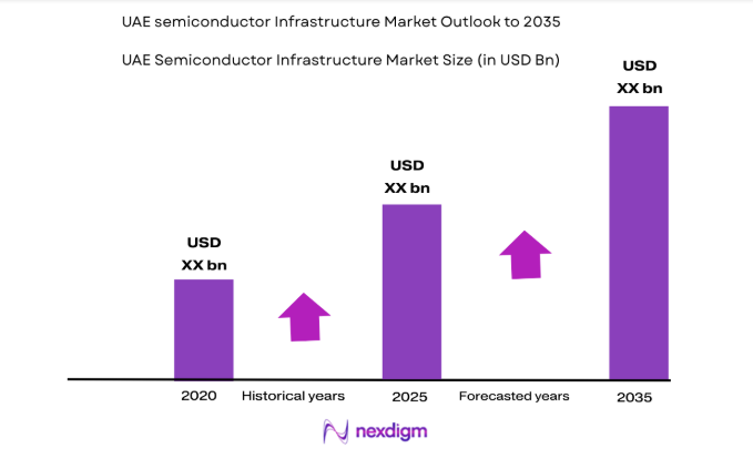
The UAE semiconductor infrastructure market reached approximately USD ~ billion based on recent industrial investment disclosures and semiconductor facility project commitments across fabrication, packaging, and cleanroom systems. Demand is driven by national advanced manufacturing programs, compound semiconductor initiatives, and infrastructure investments in high-purity utilities, advanced packaging lines, and pilot fabrication facilities. Capital deployment in semiconductor zones and technology clusters has accelerated procurement of lithography support, metrology, and ultra-clean manufacturing environments, reinforcing infrastructure expansion.
Abu Dhabi and Dubai dominate the UAE semiconductor infrastructure market due to sovereign-backed technology diversification strategies, industrial free-zone ecosystems, and proximity to advanced manufacturing investors. Abu Dhabi’s industrial zones and state-linked technology programs host compound semiconductor and advanced packaging initiatives, while Dubai’s logistics connectivity, engineering services base, and international EPC presence support semiconductor facility construction and integration. Regional collaboration with Europe and Asia semiconductor ecosystems further strengthens these cities’ infrastructure leadership.
Market Segmentation
By Product Type
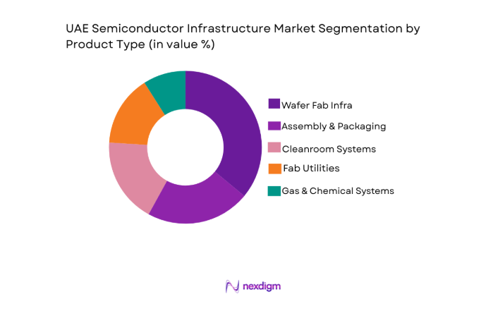
UAE semiconductor infrastructure market is segmented by product type into wafer fabrication infrastructure, assembly and packaging infrastructure, cleanroom and contamination control systems, fab utilities and process support systems, and specialty gas and chemical distribution systems. Recently, wafer fabrication infrastructure has a dominant market share due to its central role in enabling semiconductor manufacturing capacity and driving demand for advanced facility environments and utilities.
By Platform Type
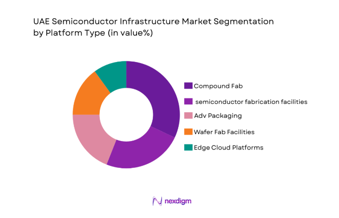
UAE semiconductor infrastructure market is segmented by platform type into wafer fabrication facilities, and legacy wafer facilities, advanced packaging and heterogeneous integration lines, compound semiconductor fabrication facilities, and semiconductor R&D and pilot line facilities. Recently, compound semiconductor fabrication facilities has a dominant market share due to national focus on power electronics and photonics manufacturing infrastructure.
Competitive Landscape
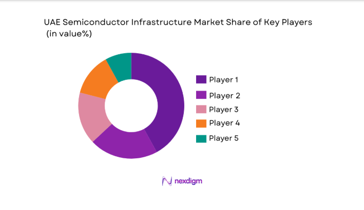
The UAE semiconductor infrastructure market shows moderate consolidation, with global semiconductor equipment leaders and EPC contractors dominating large-scale fabrication and packaging facility projects. Technology vendors provide lithography, deposition, metrology, and materials systems, while engineering firms manage fab construction, utilities integration, and cleanroom deployment. Strategic partnerships between sovereign programs and international semiconductor infrastructure suppliers strongly influence procurement patterns and project execution.
| Company Name | Establishment Year | Headquarters | Technology Focus | Market Reach | Key Products | Revenue | UAE Project Presence |
| ASML | 1984 | Netherlands | ~ | ~ | ~ | ~ | ~ |
| Applied Materials | 1967 | USA | ~ | ~ | ~ | ~ | ~ |
| Lam Research | 1980 | USA | ~ | ~ | ~ | ~ | ~ |
| Tokyo Electron | 1963 | Japan | ~ | ~ | ~ | ~ | ~ |
| Exyte | 1912 | Germany | ~ | ~ | ~ | ~ | ~ |
UAE Semiconductor Infrastructure Market Analysis
Growth Drivers
National Semiconductor Localization and Industrial Diversification Programs
The UAE semiconductor infrastructure market is expanding strongly due to sustained government-led localization initiatives that position semiconductor capability as a strategic pillar of industrial diversification and technological sovereignty. Sovereign technology programs are channeling large-scale capital into fabrication pilot lines, compound semiconductor initiatives, and advanced packaging ecosystems, requiring significant infrastructure in cleanrooms, ultra-high-purity utilities, and advanced manufacturing environments. Industrial free-zones and technology clusters are offering land, incentives, and utility frameworks tailored for semiconductor facilities, enabling faster deployment of wafer fabs and packaging lines. Strategic partnerships with global semiconductor equipment and EPC leaders are transferring facility design standards, accelerating infrastructure capability maturation. Demand for compound semiconductors in power electronics, photonics, and advanced communications is further driving specialized fab and materials infrastructure investments across the country. Integration of semiconductor initiatives with defense electronics, space, and advanced mobility sectors is creating domestic demand pull for fabrication and packaging capacity. National funding programs are supporting pilot fabrication and prototyping facilities that require full semiconductor infrastructure stacks, including metrology and process control systems. The localization push is also catalyzing supporting ecosystems such as specialty gases, ultrapure chemicals, and automation software, expanding infrastructure scope. Overall, industrial policy alignment and technology sovereignty ambitions are creating sustained multi-segment infrastructure demand across the semiconductor value chain.
Advanced Packaging and Compound Semiconductor Demand Expansion
The UAE semiconductor infrastructure market is significantly driven by rising global and regional demand for advanced packaging and compound semiconductor devices, which require specialized fabrication and assembly infrastructure distinct from conventional silicon fabs. Compound semiconductor applications in electric mobility, renewable energy conversion, and high-frequency communications are creating requirements for III-V and wide-bandgap fabrication lines, epitaxy facilities, and specialized materials handling systems. Advanced packaging technologies such as heterogeneous integration, chiplets, and photonic integration require precision assembly, bonding, and metrology environments, increasing investment in packaging infrastructure. Regional positioning as a hub for power electronics and photonics manufacturing is encouraging deployment of pilot fabs and packaging centers serving Europe, Asia, and Middle East markets. Sovereign investment entities are supporting partnerships with global compound semiconductor technology firms, accelerating infrastructure development. Integration of advanced packaging with system-level electronics manufacturing is generating additional cleanroom and automation demand. These segments require lower node complexity but higher materials and packaging precision, aligning with UAE’s industrial strategy. Growth in aerospace, defense, and telecom electronics across the region reinforces compound semiconductor demand. Consequently, infrastructure investment is shifting beyond traditional wafer fabs toward packaging and specialty semiconductor ecosystems.
Market Challenges
High Capital Intensity and Long Payback Cycles for Semiconductor Infrastructure
The UAE semiconductor infrastructure market faces a major constraint due to the extremely high capital requirements associated with establishing fabrication facilities, cleanroom environments, and ultra-pure process utilities, which can exceed several billion dollars per facility. Semiconductor fabs require sustained utilization and long operational lifecycles to achieve economic viability, creating extended payback periods that challenge investment risk tolerance. Infrastructure components such as lithography support, vacuum systems, chemical handling, and contamination control require continuous upgrades to maintain technology relevance, adding lifecycle cost pressure. For emerging semiconductor ecosystems, utilization risk is higher because domestic demand may initially be limited compared to established semiconductor regions. Securing anchor customers or technology partners is essential but complex, delaying infrastructure investment decisions. Financial exposure is amplified by technology obsolescence risk, where facility capability may lag evolving semiconductor nodes or packaging technologies. Operational costs including energy, water purification, and specialty materials supply are also significant in desert industrial environments. These cost structures necessitate sustained government support and subsidies to maintain competitiveness. Overall, capital intensity and long return horizons remain structural barriers to rapid semiconductor infrastructure scaling in the UAE.
Dependence on Imported Semiconductor Equipment and Materials Ecosystem
The UAE semiconductor infrastructure market remains heavily dependent on imported fabrication equipment, specialty materials, and advanced process technologies, creating supply chain vulnerability and strategic dependence on global semiconductor leaders. Critical infrastructure components such as lithography systems, deposition tools, metrology equipment, and ultra-pure material handling technologies are produced by a limited number of global suppliers concentrated in the US, Europe, and Japan. Export controls and technology transfer restrictions can limit access to advanced semiconductor manufacturing capabilities, constraining infrastructure sophistication. Import dependence also increases project costs due to logistics, installation complexity, and specialized engineering requirements. The absence of a mature local semiconductor materials and equipment ecosystem restricts domestic value capture from infrastructure investments. Skilled workforce dependence on international expertise further reinforces reliance on foreign vendors and engineering firms. Maintenance and lifecycle servicing of semiconductor tools require continuous international support, increasing operational risk. Supply chain disruptions or geopolitical tensions can delay infrastructure deployment timelines. Consequently, ecosystem dependency remains a structural challenge to achieving full semiconductor infrastructure autonomy in the UAE.
Opportunities
Regional Hub Positioning for Compound Semiconductor and Power Electronics Manufacturing
The UAE semiconductor infrastructure market holds strong opportunity to position itself as a regional hub for compound semiconductor and power electronics fabrication serving Europe, Middle East, and Africa demand corridors. Wide-bandgap semiconductor technologies such as SiC and GaN are experiencing rapid adoption in electric vehicles, renewable energy inverters, and high-frequency communications, creating demand for specialized fabrication lines that align with UAE industrial diversification priorities. Regional energy transition initiatives and electrification strategies provide a local demand base for power semiconductor manufacturing. Infrastructure investment in epitaxy, materials processing, and advanced packaging facilities can attract global technology partnerships seeking geographic diversification. Free-zone manufacturing ecosystems and logistics connectivity enable export-oriented semiconductor production models. Sovereign capital availability supports large-scale pilot fabs and manufacturing clusters focused on specialty semiconductors. Integration with aerospace, defense, and space electronics programs strengthens compound semiconductor demand. Lower node complexity relative to leading-edge silicon fabs reduces technology barriers while maintaining strategic relevance. Establishing a compound semiconductor hub can anchor a broader semiconductor infrastructure ecosystem in the UAE.
Public-Private Partnerships in Semiconductor R&D and Pilot Fabrication Facilities
The UAE semiconductor infrastructure market has significant opportunity in developing collaborative pilot fabrication and research facilities through public-private partnerships that combine sovereign investment with global semiconductor expertise. Pilot fabs enable prototyping, process development, and small-scale manufacturing across compound semiconductors, photonics, and advanced packaging technologies, requiring full semiconductor infrastructure stacks. Such facilities support workforce development, ecosystem formation, and technology transfer, reducing dependence on imports over time. Partnerships with international semiconductor firms and research institutions can accelerate capability building in fabrication processes and facility operations. Pilot infrastructure also enables domestic innovation in sensors, power electronics, and photonic devices aligned with national technology priorities. Integration with university research and defense electronics programs strengthens utilization and technology pipelines. Pilot fabs act as stepping-stones toward commercial manufacturing facilities while mitigating investment risk. These collaborative models align with national industrial policy frameworks and sovereign investment strategies. Consequently, public-private semiconductor infrastructure initiatives represent a major growth opportunity in the UAE.
Future Outlook
The UAE semiconductor infrastructure market is expected to expand steadily as national industrial diversification strategies continue to prioritize advanced manufacturing and semiconductor capability development. Growth will be supported by compound semiconductor demand, advanced packaging adoption, and sovereign investment in pilot fabrication ecosystems. Technology partnerships with global semiconductor leaders will accelerate infrastructure maturity, while regulatory incentives and free-zone manufacturing clusters attract fabrication and packaging projects. Regional electronics demand and energy transition initiatives will further strengthen semiconductor infrastructure deployment.
Major Players
- ASML
- Applied Materials
- Lam Research
- Tokyo Electron
- KLA Corporation
- SCREEN Holdings
- ASM International
- Advantest
- Teradyne
- Air Liquide
- Linde
- Entegris
- Exyte
- Jacobs
- Bechtel
Key Target Audience
- Semiconductor manufacturing companies
- Electronics and advanced manufacturing firms
- Sovereign wealth funds and investment authorities
- Government and regulatory bodies
- Venture capital and private equity firms
- Industrial infrastructure developers
- Defense and aerospace electronics firms
- Energy and power electronics companies
Research Methodology
Step 1: Identification of Key Variables
Key variables influencing the UAE semiconductor infrastructure market were identified through analysis of fabrication facility investments, semiconductor policy frameworks, and industrial diversification programs. Supply-side factors such as equipment procurement, cleanroom capacity, and utility infrastructure were mapped alongside demand drivers from electronics and energy sectors.
Step 2: Market Analysis and Construction
The market was constructed by aggregating infrastructure investments across fabrication, packaging, cleanroom, and process support systems deployed in semiconductor projects. Facility cost benchmarks, equipment intensity ratios, and project deployment timelines were applied to derive market structure and segment distribution across system types and end-users.
Step 3: Hypothesis Validation and Expert Consultation
Market assumptions were validated through consultation with semiconductor equipment suppliers, EPC contractors, and regional industrial development stakeholders. Technology deployment patterns, infrastructure cost structures, and ecosystem maturity levels were cross-verified to ensure realistic representation of UAE semiconductor infrastructure dynamics.
Step 4: Research Synthesis and Final Output
All validated data and insights were synthesized into a structured analysis covering market size, segmentation, competitive landscape, and strategic outlook. Consistency checks ensured alignment between infrastructure investments, policy drivers, and semiconductor technology adoption trajectories shaping the UAE market.
- Executive Summary
- Research Methodology (Definitions, Scope, Industry Assumptions, Market Sizing Approach, Primary & Secondary Research Framework, Data Collection & Verification Protocol, Analytic Models & Forecast Methodology, Limitations & Research Validity Checks)
- Market Definition and Scope
- Value Chain & Stakeholder Ecosystem
- Regulatory / Certification Landscape
- Sector Dynamics Affecting Demand
- Strategic Initiatives & Infrastructure Growth

- Growth Drivers
National semiconductor localization and industrial diversification initiatives
Rising demand for advanced packaging and compound semiconductor capacity
Strategic investment zones and incentives for high-tech manufacturing - Market Challenges
High capital intensity and long payback cycles for fab infrastructure
Dependence on imported critical equipment and materials
Skills and ecosystem maturity gaps in advanced node manufacturing - Market Opportunities
Regional hub positioning for compound semiconductor and power electronics fabs
Public-private partnerships in semiconductor R&D and pilot lines
Expansion of advanced packaging and heterogeneous integration facilities - Trends
Shift toward modular and scalable fab construction approaches
Integration of smart manufacturing and automation in fabs
Growth in compound semiconductor and specialty device fabrication
Adoption of digital twin and predictive maintenance in facilities
Increasing focus on sustainability and resource efficiency in fabs - Government Regulations & Defense Policy
Strategic technology investment and localization policies
Export control and technology transfer compliance frameworks
Industrial free-zone incentives for semiconductor manufacturing - SWOT Analysis
- Stakeholder and Ecosystem Analysis
- Porter’s Five Forces Analysis
- Competition Intensity and Ecosystem Mapping
- By Market Value, 2020-2025
- By Installed Units, 2020-2025
- By Average System Price, 2020-2025
- By System Complexity Tier, 2020-2025
- By System Type (In Value%)
Wafer Fabrication Facilities
Assembly, Packaging, and Test Infrastructure
Cleanroom and Contamination Control Systems
Fab Utilities and Process Support Systems
Specialty Gas and Chemical Distribution Systems - By Platform Type (In Value%)
300mm Wafer Fabs
200mm and Legacy Fabs
Advanced Packaging and Heterogeneous Integration Lines
Compound Semiconductor Fabs
R&D and Pilot Line Facilities - By Fitment Type (In Value%)
Greenfield Fab Installations
Brownfield Expansion and Retrofit
Modular Fab Units
Turnkey EPC Fab Solutions
Equipment-Level Integration Upgrades - By EndUser Segment (In Value%)
Foundry Operators
Integrated Device Manufacturers
OSAT Providers
Research Institutes and Universities
Government Semiconductor Programs - By Procurement Channel (In Value%)
Direct OEM Procurement
EPC and Turnkey Contractors
Government Tender Programs
Technology Partnerships and JVs
Distributor and Integrator Networks - By Material / Technology (in Value %)
EUV and Advanced Lithography Infrastructure
Deposition and Etch Process Systems
Metrology and Inspection Systems
Ultra-High Purity Materials Handling
Automation and Smart Fab Software
- Market structure and competitive positioning
Market share snapshot of major players - Cross Comparison Parameters (Technology Node Capability, Fab Construction Model, Packaging Integration Capability, Automation Level, Local Partnership Presence, Project Scale, End-to-End Service Scope, Sustainability Compliance, Aftermarket Support)
- SWOT Analysis of Key Competitors
- Pricing & Procurement Analysis
- Key Players
ASML
Applied Materials
Lam Research
Tokyo Electron
KLA Corporation
SCREEN Holdings
ASM International
Advantest
Teradyne
Air Liquide
Linde
Entegris
Exyte
Jacobs
Bechtel
- Foundries prioritizing scalable 300mm and advanced packaging capacity
- IDMs investing in localized specialty and power semiconductor lines
- OSAT providers expanding heterogeneous integration capabilities
- Public R&D entities building pilot fabs and prototyping infrastructure
- Forecast Market Value, 2026-2035
- Forecast Installed Units, 2026-2035
- Price Forecast by System Tier, 2026-2035
- Future Demand by Platform, 2026-2035


 Request a Sample
 Ask for Customization
 Get a Quote
 Enquire Now