
 Download PDF
 Download PDF
Market Overview
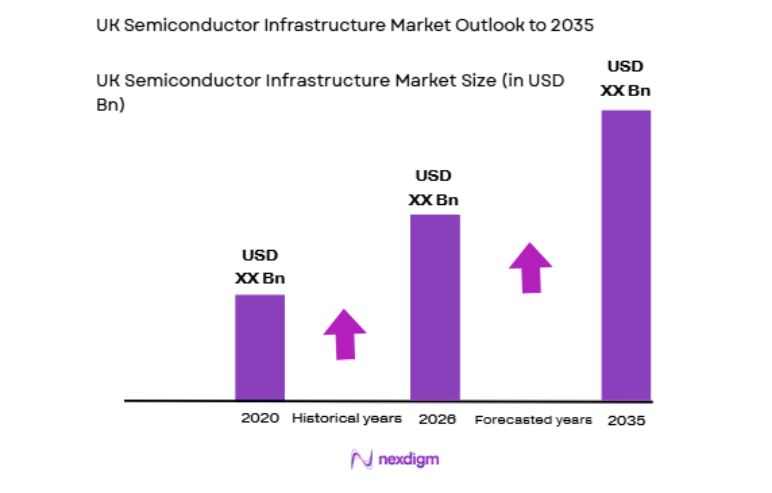
The UK semiconductor infrastructure market demonstrates strong institutional and industrial backing, with public programs and private capital collectively supporting fabrication, advanced packaging, testing, and materials processing ecosystems. Based on a recent historical assessment, the market size is estimated at approximately USD ~ billion, driven by strategic domestic capacity expansion, compound semiconductor leadership, and defense-linked electronics demand. National semiconductor strategy funding and regional innovation clusters further stimulate infrastructure investments across cleanroom facilities, equipment procurement, and specialty material processing capabilities.
Key geographic concentration is observed in South Wales, Cambridge, and Scotland due to established compound semiconductor clusters, research excellence, and skilled workforce availability. These regions host advanced packaging, photonics, and wafer processing infrastructure anchored by academic-industry collaboration and government-supported technology parks. Proximity to aerospace, defense electronics, and automotive semiconductor supply chains reinforces regional dominance, while export-oriented photonics and compound semiconductor manufacturing strengthens global integration and sustained infrastructure utilization across the United Kingdom.
Market Segmentation
By Product Type
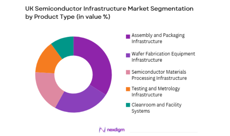
UK Semiconductor Infrastructure Market is segmented by product type into wafer fabrication equipment infrastructure, assembly and packaging infrastructure, semiconductor materials processing infrastructure, testing and metrology infrastructure, and cleanroom and facility systems. Recently, assembly and packaging infrastructure has a dominant market share due to strong domestic specialization in compound semiconductor packaging, photonics integration, and advanced heterogeneous integration technologies. The United Kingdom hosts several high-value packaging and photonics manufacturing clusters, particularly in South Wales and Scotland, supported by government innovation funding and academic partnerships. Increasing demand for advanced packaging in aerospace, telecom, and defense electronics further strengthens this segment. Compared with wafer fabrication, packaging requires lower capital intensity and aligns with UK industrial strengths in precision engineering and photonics integration. The presence of established packaging firms and pilot lines accelerates commercialization, attracting infrastructure investments.
By End-Use Industry
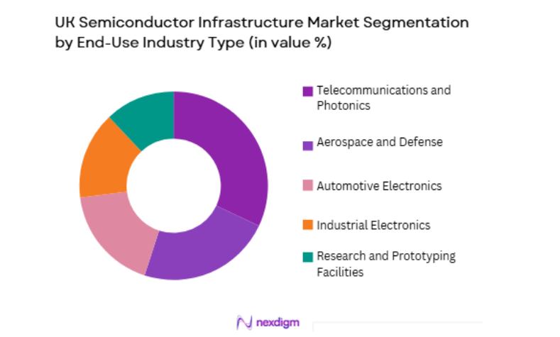
UK Semiconductor Infrastructure Market is segmented by end-use industry into telecommunications and photonics, automotive electronics, aerospace and defense, industrial electronics, and research and prototyping facilities. Recently, telecommunications and photonics has a dominant market share due to the United Kingdom’s global leadership in compound semiconductors, optical communications, and photonic integrated circuits manufacturing. Strong export demand for optical components and telecom infrastructure modules sustains fabrication, packaging, and testing infrastructure utilization. National investments in optical networking, quantum photonics, and 5G/6G technologies further expand capacity requirements. Academic-industry clusters in Cambridge and South Wales specialize in photonic devices, reinforcing ecosystem concentration. Compared with automotive or industrial electronics, photonics requires specialized compound semiconductor processing infrastructure aligned with UK technological strengths.
Competitive Landscape
The UK semiconductor infrastructure market is moderately consolidated, characterized by specialized compound semiconductor, photonics, and packaging leaders alongside global equipment and materials firms operating through local facilities and partnerships. Domestic champions dominate advanced packaging and compound semiconductor processing, while multinational equipment providers supply fabrication and metrology infrastructure.
| Company Name | Establishment Year | Headquarters | Technology Focus | Market Reach | Key Products | Revenue | UK Semiconductor Specialization |
| IQE plc | 1988 | Cardiff, UK | ~ | ~ | ~ | ~ | ~ |
| Newport Wafer Fab | 1982 | Newport, UK | ~ | ~ | ~ | ~ | ~ |
| Oxford Instruments | 1959 | Oxford, UK | ~ | ~ | ~ | ~ | ~ |
| SPTS Technologies | 2009 | Newport, UK | ~ | ~ | ~ | ~ | ~ |
| Clas-SiC Wafer Fab | 2017 | Lochgelly, UK | ~ | ~ | ~ | ~ | ~ |
UK Semiconductor Infrastructure Market Analysis
Growth Drivers
National Semiconductor Strategy and Sovereign Manufacturing Investment
The United Kingdom accelerates semiconductor infrastructure development through coordinated national funding, strategic technology programs, and incentives supporting fabrication, packaging, testing, materials processing, and facility upgrades across regional clusters and supply chains. Government commitments prioritize compound semiconductor leadership, photonics manufacturing, and advanced packaging capabilities aligned with defense, telecom, and automotive demand. Public-private partnerships channel investment into pilot lines, cleanrooms, and process equipment modernization supporting commercialization readiness. Regional innovation hubs expand infrastructure capacity while strengthening workforce development and technology transfer ecosystems. Sovereign capability goals reduce import dependency in strategic electronics supply chains. Defense electronics modernization and secure communications programs sustain infrastructure utilization across fabrication and packaging segments. Export-oriented photonics manufacturing attracts foreign investment and collaborative infrastructure expansion. Academic-industry research centers anchor innovation-led infrastructure upgrades across regions. Supply chain localization initiatives strengthen domestic materials processing and testing capacity.
Private Capital Inflows and Compound Semiconductor Cluster Expansion
Venture capital, corporate investment, and strategic partnerships increasingly support United Kingdom semiconductor infrastructure, particularly in compound semiconductor, photonics, and advanced packaging segments aligned with national technological strengths and export markets. Growth in optical communications, sensing, and power electronics markets attracts infrastructure investment into wafer processing and packaging facilities. Cluster-based ecosystems in South Wales and Cambridge foster commercialization pathways requiring scalable infrastructure expansion. Corporate alliances with global equipment suppliers accelerate technology deployment in domestic facilities. Private funding complements public programs, enabling faster pilot-to-production transitions across infrastructure assets. Start-up growth in photonics and quantum technologies increases demand for prototyping and testing infrastructure. Industrial electronics and aerospace applications broaden compound semiconductor utilization. International customers seeking specialized photonics manufacturing support domestic capacity expansion. Local supply chain partnerships enhance materials and metrology infrastructure resilience.
Market Challenges
Limited Leading-Edge Wafer Fabrication Capacity and Capital Intensity Constraints
The United Kingdom faces structural limitations in leading-edge semiconductor fabrication infrastructure due to high capital requirements, limited domestic demand scale, and global competition from established mega-fabs concentrated in Asia and North America. Domestic infrastructure specialization in compound semiconductors and packaging constrains diversification into advanced silicon nodes. High equipment costs and cleanroom investments restrict rapid capacity expansion. Limited wafer volumes reduce economies of scale for fabrication facilities. Dependence on imported equipment and materials increases supply chain vulnerability. Skilled workforce shortages in advanced process engineering constrain facility upgrades. Fragmented funding across regions slows coordinated infrastructure scaling. Global semiconductor cycles create investment uncertainty for domestic fabs. Export-focused compound semiconductor segments face demand volatility. These factors collectively limit comprehensive fabrication infrastructure development nationally.
Fragmented Ecosystem Coordination and Commercialization Scaling Barriers
The UK semiconductor infrastructure ecosystem includes universities, research centers, start-ups, and specialized firms, but fragmented coordination across stakeholders limits efficient infrastructure utilization and large-scale commercialization readiness across segments. Technology transfer pathways from research to manufacturing remain uneven across regions. Infrastructure sharing mechanisms between academia and industry require stronger integration frameworks. Start-ups face barriers accessing pilot-scale fabrication and packaging facilities. Regional funding disparities create uneven infrastructure maturity. Commercial scaling timelines extend due to certification and qualification requirements. Supply chain partnerships remain fragmented across materials and testing providers. Market access for emerging semiconductor products requires expanded manufacturing capacity. Coordination gaps reduce investor confidence in infrastructure scalability. National strategy alignment across stakeholders remains evolving. These structural coordination challenges constrain ecosystem efficiency.
Opportunities
Advanced Packaging and Heterogeneous Integration Infrastructure Leadership
The United Kingdom can establish global leadership in advanced semiconductor packaging infrastructure by leveraging compound semiconductor expertise, photonics integration capabilities, and precision engineering strengths across regional clusters and industry collaborations. Demand for heterogeneous integration in telecom, automotive, and defense electronics drives packaging capacity expansion. Photonic integrated circuit manufacturing requires specialized packaging infrastructure aligned with domestic strengths. Lower capital intensity compared with wafer fabrication improves investment feasibility. Export-oriented photonics modules support sustained packaging utilization. Government programs already prioritize packaging technology innovation. Academic-industry research accelerates commercialization of packaging techniques. Global semiconductor firms seek specialized packaging partners. Supply chain localization enhances domestic packaging ecosystems. These factors position advanced packaging infrastructure as a strategic growth opportunity nationally.
Compound Semiconductor and Power Electronics Fabrication Expansion
Growing global demand for power electronics, sensing, and photonics devices enables the United Kingdom to expand compound semiconductor fabrication infrastructure leveraging existing clusters, skilled workforce, and established industrial partnerships across regions and export markets. Electric vehicles and renewable energy systems increase SiC and GaN device demand. Aerospace and defense electronics require high-performance compound semiconductors. Domestic firms already possess epitaxy and wafer processing expertise. Infrastructure expansion builds on existing facilities rather than greenfield fabs. Government incentives target compound semiconductor scale-up. International partnerships support technology transfer and investment. Materials and metrology ecosystems already exist locally. Export demand sustains fabrication utilization. These drivers create strong opportunities for compound semiconductor infrastructure expansion nationwide.
Future Outlook
The UK semiconductor infrastructure market is expected to expand steadily over the next five years, supported by national semiconductor strategy funding, private investment, and growing compound semiconductor demand. Advanced packaging, photonics manufacturing, and power electronics fabrication will drive infrastructure upgrades. Regional clusters will strengthen through academic-industry collaboration and supply chain localization. Regulatory support and defense electronics programs will sustain long-term infrastructure utilization.
Major Players
- Arm Holdings
- IQE plc
- Nexperia UK
- Vishay Newport
- Paragraf
- EnSilica
- Pragmatic Semiconductor
- Dialog Semiconductor
- SmartKem
- TeraView
- Dynex Semiconductor
- Graphcore
- Plessey Semiconductors
- IceMOS Technology
- Marvell Technology
Key Target Audience
- Semiconductor fabrication plants
- Integrated device manufacturers
- Foundry and wafer production companies
- AI and HPC infrastructure providers
- Electronics and telecom equipment manufacturers
- Government and regulatory bodies
- Investments and venture capitalist firms
- Defense and aerospace system manufacturers
Research Methodology
Step 1: Identification of Key Variables
Key infrastructure variables including fabrication capacity, packaging capability, equipment deployment, materials processing, and regional cluster concentration were identified through industry reports, policy documents, and company disclosures. Demand drivers across telecom, automotive, defense, and photonics sectors were mapped to infrastructure requirements. Technology specialization trends in compound semiconductors and packaging were also incorporated.
Step 2: Market Analysis and Construction
Market size and segmentation were constructed using secondary data from government semiconductor strategy releases, company financials, trade associations, and infrastructure investment announcements. Regional cluster capacities and facility expansions were benchmarked. Product and end-use segmentation shares were estimated based on infrastructure utilization patterns and industry demand alignment.
Step 3: Hypothesis Validation and Expert Consultation
Findings were validated through consultations with semiconductor engineers, industry analysts, and infrastructure specialists across fabrication, packaging, and photonics segments. Regional cluster assessments and technology specialization assumptions were cross-checked with expert insights. Demand-side drivers and infrastructure constraints were refined based on practitioner feedback.
Step 4: Research Synthesis and Final Output
All validated data points were synthesized into a structured market model integrating infrastructure capacity, demand drivers, segmentation shares, and competitive positioning. Qualitative insights on ecosystem dynamics and policy influence were incorporated. Final outputs were reviewed for consistency with national semiconductor strategy objectives and industry structure.
- Executive Summary
- Research Methodology (Definitions, Scope, Industry Assumptions, Market Sizing Approach, Primary & Secondary Research Framework, Data Collection & Verification Protocol, Analytic Models & Forecast Methodology, Limitations & Research Validity Checks)
- Market Definition and Scope
- Value Chain & Stakeholder Ecosystem
- Regulatory / Certification Landscape
- Sector Dynamics Affecting Demand

- Growth Drivers
Expansion of compound semiconductor clusters in South Wales and Scotland
Public funding initiatives supporting domestic semiconductor capacity
Rising demand for advanced packaging and heterogeneous integration facilities - Market Challenges
High capital intensity and long payback cycles for fab infrastructure
Dependence on imported lithography and process equipment ecosystems
Skills shortages in semiconductor facility engineering and operations - Market Opportunities
Development of compound semiconductor and photonics fabs
Localization of advanced packaging and test capabilities
Public–private partnerships for resilient semiconductor supply chains - Trends
Shift toward compound semiconductor manufacturing platforms
Integration of automation and digital twin technologies in fabs
Growth of heterogeneous integration and advanced packaging lines - Government regulations
UK National Semiconductor Strategy funding frameworks
Export control and foreign investment screening in semiconductor assets
Environmental and cleanroom compliance standards for fabs - SWOT analysis
- Porters Five forces
- By Market Value, 2020-2025
- By Installed Units, 2020-2025
- By Average System Price, 2020-2025
- By System Complexity Tier, 2020-2025
- By System Type (In Value%)
Wafer Fabrication Facility Infrastructure
Assembly and Packaging Facility Systems
Semiconductor Testing and Metrology Infrastructure
Cleanroom and Environmental Control Systems
Materials Handling and Automation Systems - By Platform Type (In Value%)
IDM Manufacturing Facilities
Pure-play Foundry Facilities
OSAT Packaging and Test Facilities
R&D and Pilot Line Facilities
Compound Semiconductor Fabs - By Fitment Type (In Value%)
New Fab Greenfield Installations
Brownfield Fab Expansions
Tool Retrofit and Modernization
Facility Automation Upgrades
Cleanroom Capacity Enhancements - By End User Segment (In Value%)
Integrated Device Manufacturers
Fabless Semiconductor Firms
Foundry Operators
- Market Share Analysis
- Cross Comparison Parameters (Facility Type Coverage, Technology Node Capability, Packaging Infrastructure Scope, Cleanroom Class Expertise, EPC Delivery Capability, Automation and Robotics Integration)
- SWOT Analysis of Key Competitors
- Pricing & Procurement Analysis
- Key Players
IQE plc
Oxford Instruments plc
Edwards Vacuum
SPTS Technologies
CPI TMD Technologies
Clas-SiC Wafer Fab
Nexperia UK
Teledyne e2v
TT Electronics Semelab
Compound Semiconductor Technologies Global
Cambridge GaN Devices
Pragmatic Semiconductor
Paragraf
Kelvin Nanotechnology
Semefab
- Defense and aerospace electronics firms driving secure domestic fab demand
- Research institutes shaping pilot-line and prototyping infrastructure needs
- IDMs investing in compound semiconductor capacity expansion
- Fabless firms leveraging local packaging and test ecosystems
- Forecast Market Value, 2026-2035
- Forecast Installed Units, 2026-2035
- Price Forecast by System Tier, 2026-2035
- Future Demand by Platform, 2026-2035


 Request a Sample
 Ask for Customization
 Get a Quote
 Enquire Now