
 Download PDF
 Download PDF
Market Overview
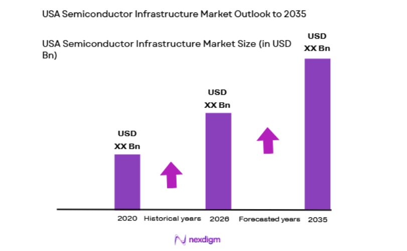
The USA semiconductor infrastructure market reached approximately USD ~ billion based on a recent historical assessment, driven by accelerated domestic fab expansion, advanced node transition, and sustained public incentives under federal industrial policy frameworks. Capital intensity across wafer fabrication equipment, materials processing, and cleanroom facility systems remained elevated due to leading-edge logic and memory investments reported by the Semiconductor Industry Association and U.S. Department of Commerce.
Dominance within the USA semiconductor infrastructure landscape is concentrated in states with established fabrication ecosystems, skilled engineering labor pools, and proximity to design clusters and advanced research institutions. Arizona, Texas, and New York lead due to large-scale fabrication campuses, supply chain clustering, and sustained public infrastructure support, while California maintains influence through equipment innovation, venture funding networks, and semiconductor design headquarters concentration.
Market Segmentation
By Product Type
USA Semiconductor Infrastructure market is segmented by product type into wafer fabrication equipment infrastructure, semiconductor materials processing infrastructure, testing and metrology infrastructure, assembly and packaging infrastructure, and cleanroom and facility systems. Recently, wafer fabrication equipment infrastructure has a dominant market share due to strong capital allocation toward advanced logic and memory fabrication lines, sustained domestic manufacturing incentives, and the need for extreme ultraviolet lithography readiness across leading-edge nodes. Equipment-intensive process scaling, yield optimization demands, and domestic capacity reshoring policies further concentrate spending in lithography, etch, deposition, and process control systems.

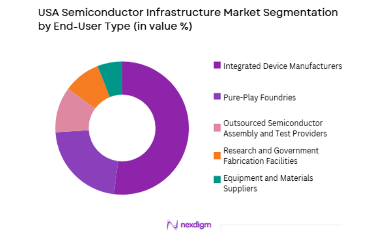
By End User
USA Semiconductor Infrastructure market is segmented by end user into integrated device manufacturers, pure-play foundries, outsourced semiconductor assembly and test providers, research and government fabrication facilities, and equipment and materials suppliers. Recently, integrated device manufacturers has a dominant market share due to vertically integrated production strategies, domestic capacity localization mandates, and large-scale capital programs targeting advanced logic, memory, and specialty semiconductor manufacturing. Major U.S. semiconductor firms continue expanding proprietary fabs to secure supply continuity, intellectual property protection, and process differentiation, resulting in disproportionately higher infrastructure spending relative to other user groups.
Competitive Landscape
The USA semiconductor infrastructure market exhibits a concentrated competitive structure dominated by global equipment leaders and domestic technology suppliers with deep process expertise and long-term relationships with fabrication operators. High technological barriers, qualification cycles, and capital intensity limit new entrants, reinforcing the influence of established firms across lithography support, deposition, metrology, and facility systems integration. Strategic partnerships with domestic fabs and government-backed manufacturing programs further strengthen incumbent positioning.
| Company Name | Establishment Year | Headquarters | Technology Focus | Market Reach | Key Products | Revenue | Primary Infrastructure Segment |
| Applied Materials | 1967 | USA | ~ | ~ | ~ | ~ | ~ |
| Lam Research | 1980 | USA | ~ | ~ | ~ | ~ | ~ |
| KLA Corporation | 1976 | USA | ~ | ~ | ~ | ~ | ~ |
| Teradyne | 1960 | USA | ~ | ~ | ~ | ~ | ~ |
| Entegris | 1966 | USA | ~ | ~ | ~ | ~ | ~ |
USA Semiconductor Infrastructure Market Analysis
Growth Drivers
Domestic Semiconductor Manufacturing Incentives and Capacity Expansion Programs
The implementation of large-scale federal semiconductor manufacturing incentives has catalyzed unprecedented capital deployment into domestic fabrication infrastructure across the United States, directly stimulating demand for wafer fabrication equipment, cleanroom construction systems, advanced materials processing tools, and metrology platforms. Public funding frameworks tied to domestic capacity expansion have reduced investment risk for semiconductor manufacturers while requiring localized production commitments that translate into multibillion-dollar fabrication campus developments across multiple states. These policy-driven expansions create sustained multi-year procurement pipelines for infrastructure suppliers spanning front-end processing equipment, facility automation, and contamination-controlled environments necessary for advanced node production. Integrated device manufacturers and foundry operators are prioritizing domestic footprint growth to secure supply resilience and geopolitical risk mitigation, reinforcing infrastructure demand concentration within the national ecosystem. The scale and technological sophistication of new fabrication facilities necessitate leading-edge lithography readiness, process control precision, and environmental regulation compliance, increasing per-fab infrastructure intensity compared to previous technology generations. Workforce development programs and regional semiconductor clusters further enhance infrastructure absorption capacity by aligning talent supply with fabrication deployment schedules.
Transition Toward Advanced Nodes and Heterogeneous Integration Architectures
The semiconductor industry’s progression toward advanced process nodes and heterogeneous integration technologies is significantly increasing infrastructure complexity and capital intensity requirements across fabrication and packaging environments in the United States. Sub-5-nanometer manufacturing and advanced transistor architectures demand highly precise lithography compatibility, advanced deposition chemistries, and next-generation etch and metrology capabilities, driving accelerated replacement and expansion of wafer fabrication infrastructure. Simultaneously, heterogeneous integration approaches combining logic, memory, and specialized chips within advanced packaging configurations are expanding infrastructure demand beyond traditional front-end processes into high-density interconnect, wafer-level packaging, and three-dimensional assembly facilities. These technology shifts require upgraded contamination control systems, ultra-clean materials handling environments, and real-time process monitoring infrastructure across fabrication ecosystems. U.S. semiconductor manufacturers are investing in integrated fab-packaging campuses to support advanced system architectures, thereby increasing aggregate infrastructure spending per production unit. Design-manufacturing co-optimization strategies also necessitate tighter process control tolerances and sophisticated inspection infrastructure across production lines. Continuous node shrink and architectural innovation cycles shorten equipment obsolescence timelines, accelerating reinvestment rates in semiconductor infrastructure assets.
Market Challenges
Extreme Capital Intensity and Long Payback Cycles in Fabrication Infrastructure
Semiconductor fabrication infrastructure requires exceptionally high upfront capital expenditure across equipment procurement, cleanroom construction, utilities integration, and facility automation systems, creating financial barriers and extended payback horizons for manufacturers operating within the United States. Advanced node fabrication plants demand multibillion-dollar investments before commercial output begins, with infrastructure components representing a substantial share of total project cost due to precision environmental requirements and specialized process equipment. Long construction timelines and technology qualification phases delay revenue realization, exposing investors to market demand fluctuations and technology obsolescence risks during deployment periods. Infrastructure suppliers must maintain large research and production capacity without guaranteed short-term returns, amplifying financial exposure across the value chain. Financing complexity increases when projects depend on public incentives contingent on domestic production milestones and compliance criteria, creating execution risk for infrastructure investments. High depreciation costs associated with rapidly evolving process equipment further compress return on invested capital for fabrication operators. Smaller semiconductor firms and emerging manufacturers face disproportionate difficulty accessing capital for infrastructure build-out, reinforcing industry concentration. Cyclical semiconductor demand patterns additionally create utilization volatility, challenging infrastructure cost recovery assumptions.
Supply Chain Complexity and Critical Equipment Dependency Risks
Semiconductor infrastructure deployment in the United States depends on highly specialized global supply chains for advanced equipment components, ultra-pure materials, precision sensors, and environmental control systems, exposing fabrication projects to disruption risks and procurement bottlenecks. Many critical subsystems used in lithography compatibility, vacuum processing, and contamination control rely on limited global suppliers with long manufacturing lead times and stringent qualification requirements. Export control regulations and geopolitical trade restrictions can constrain access to certain advanced manufacturing technologies or components, complicating infrastructure planning and increasing compliance costs for domestic fabrication operators. Infrastructure projects require synchronized delivery of thousands of precision components, and delays in any subsystem can postpone entire fab commissioning schedules, escalating capital costs. Domestic localization efforts face technical and capacity challenges in replicating established global supplier capabilities, slowing supply chain diversification. Equipment customization for advanced node processes further lengthens production and installation timelines, reducing flexibility in infrastructure deployment. Logistics complexity associated with transporting sensitive semiconductor equipment also increases project risk and insurance costs.
Opportunities
Advanced Packaging and Heterogeneous Integration Infrastructure Expansion
The accelerating adoption of advanced packaging and heterogeneous integration technologies across high-performance computing, artificial intelligence, and defense semiconductor applications is creating substantial infrastructure expansion opportunities within the United States semiconductor ecosystem. Advanced packaging facilities require specialized assembly, wafer-level processing, and high-density interconnect infrastructure distinct from conventional front-end fabrication environments, opening new investment segments for equipment and facility suppliers. Domestic initiatives to localize complete semiconductor value chains are increasing funding and policy support for advanced packaging capacity alongside fabrication expansion programs. Integrated chiplet architectures and three-dimensional stacking technologies demand precision alignment systems, thermal management infrastructure, and advanced inspection capabilities, stimulating equipment innovation and deployment. U.S. semiconductor manufacturers are integrating packaging infrastructure within fabrication campuses to optimize performance and supply chain control, increasing overall infrastructure intensity. Defense and high-reliability semiconductor programs further prioritize domestic packaging capabilities to ensure secure electronics production. Research institutions and government labs are expanding pilot-scale packaging facilities, supporting ecosystem development and workforce specialization.
Domestic Equipment and Materials Supply Chain Localization Initiatives
National strategies aimed at strengthening domestic semiconductor supply chains are creating significant opportunities for localized equipment manufacturing, materials processing infrastructure, and facility systems integration across the United States. Policymakers and industry stakeholders are prioritizing reduced reliance on external suppliers for critical semiconductor production inputs, encouraging domestic development of process equipment components, ultra-pure materials, and fabrication support systems. Incentive programs and public funding mechanisms support expansion of domestic infrastructure suppliers capable of serving advanced fabrication requirements, fostering new industrial capacity. Localization efforts enable closer collaboration between equipment manufacturers and fabrication operators, accelerating innovation cycles and customization efficiency. Regional semiconductor clusters integrating suppliers, manufacturers, and research institutions enhance ecosystem resilience and infrastructure deployment speed. Domestic sourcing reduces logistics risk, compliance complexity, and geopolitical exposure associated with global supply chains. Emerging U.S. firms specializing in niche semiconductor infrastructure technologies gain market entry opportunities under localization frameworks. Workforce development aligned with domestic manufacturing expansion strengthens long-term infrastructure capability.
Future Outlook
The USA semiconductor infrastructure market is expected to expand steadily over the next five years as domestic fabrication programs transition from construction to production phases. Advanced node migration and heterogeneous integration will elevate infrastructure intensity per facility. Continued regulatory incentives and supply chain localization policies will sustain capital inflows. Demand from artificial intelligence, automotive electronics, and defense semiconductors will reinforce infrastructure modernization.
Major Players
- Applied Materials
- Lam Research
- KLA Corporation
- Teradyne
- Entegris
- ASML USA
- Tokyo Electron America
- Onto Innovation
- Axcelis Technologies
- Veeco Instruments
- Brooks Automation
- MKS Instruments
- Cohu
- FormFactor
- Kulicke and Soffa
Key Target Audience
- Semiconductor integrated device manufacturers
- Pure-play foundries
- Outsourced semiconductor assembly and test providers
- Equipment manufacturers
- Materials suppliers
- Investments and venture capitalist firms
- Government and regulatory bodies
- Defense electronics manufacturers
Research Methodology
Step 1: Identification of Key Variables
Key infrastructure segments, end-user categories, technology nodes, and investment flows were mapped across the USA semiconductor ecosystem. Policy incentives, fabrication capacity announcements, and equipment spending patterns were identified as primary analytical variables.
Step 2: Market Analysis and Construction
Segment-level revenue pools were constructed using fabrication capital expenditure data, equipment supplier financials, and public manufacturing investment disclosures. Infrastructure allocation ratios were derived across product and end-user segments.
Step 3: Hypothesis Validation and Expert Consultation
Industry experts across semiconductor equipment, fabrication operations, and policy institutions validated infrastructure demand drivers, investment cycles, and supply chain dynamics. Assumptions were refined using triangulated qualitative insights.
Step 4: Research Synthesis and Final Output
Quantitative estimates and qualitative drivers were synthesized into a structured market framework. Segment shares, competitive landscape, and growth dynamics were finalized through consistency checks and scenario alignment.
- Executive Summary
- Research Methodology (Definitions, Scope, Industry Assumptions, Market Sizing Approach, Primary & Secondary Research Framework, Data Collection & Verification Protocol, Analytic Models & Forecast Methodology, Limitations & Research Validity Checks)
- Market Definition and Scope
- Value Chain & Stakeholder Ecosystem
- Regulatory / Certification Landscape
- Sector Dynamics Affecting Demand

- Growth Drivers
Federal incentives accelerating domestic fab construction and equipment orders
Rising AI and data center demand increasing advanced node and packaging capacity needs
Supply chain resilience priorities driving reshoring of critical semiconductor production - Market Challenges
Long tool lead times and constrained supply for lithography and advanced process equipment
High power, water, and permitting requirements slowing fab site readiness and timelines
Skilled labor shortages across construction, facilities, and process engineering roles - Market Opportunities
Advanced packaging buildouts for chiplets, 2.5D, and 3D integration ecosystems
Facility upgrades for energy efficiency, water recycling, and high uptime utilities
Expansion of secure and trusted manufacturing for defense and critical infrastructure chips - Trends
Acceleration of fab mega sites with clustered supplier and ecosystem development
Greater adoption of automation and digital twins for fab construction and ramp
Increased focus on contamination control and ultra high purity chemical delivery systems - Government regulations
- SWOT analysis
- Porters Five forces
- By Market Value, 2020-2025
- By Installed Units, 2020-2025
- By Average System Price, 2020-2025
- By System Complexity Tier, 2020-2025
- By System Type (In Value%)
Wafer Fabrication Equipment Infrastructure
Assembly and Packaging Infrastructure
Testing and Metrology Infrastructure
Semiconductor Materials Processing Infrastructure
Cleanroom and Facility Systems - By Platform Type (In Value%)
Logic and Advanced Node Fabs
Memory Manufacturing Facilities
Foundry and IDM Mega Fab Campuses
Advanced Packaging and OSAT Sites
R and D Pilot Lines and Prototyping Fabs - By Fitment Type (In Value%)
Greenfield Fab Construction Projects
Brownfield Fab Expansion and Upgrade
Tool Retrofit and Productivity Enhancement
Modular Cleanroom Add Ons
Utilities and Facility Modernization Programs - By End User Segment (In Value%)
Integrated Device Manufacturers
Pure Play Foundries
OSAT and Advanced Packaging Providers
- Market Share Analysis
- Cross Comparison Parameters (Process tool portfolio depth, Advanced packaging capability, EPC and fab build execution strength, Service footprint and uptime support, Compliance and trusted supply chain readiness, Installed base and customer relationships)
- SWOT Analysis of Key Competitors
- Pricing & Procurement Analysis
- Key Players
Applied Materials
Lam Research
KLA Corporation
ASML
Tokyo Electron
ASM International
Veeco Instruments
Teradyne
Advantest
Ultra Clean Holdings
MKS Instruments
Entegris
Air Liquide
Linde
Jacobs
- IDMs prioritize vertical integration, yield ramp speed, and secure supply for critical products
- Foundries focus on leading edge tool availability, scale economics, and customer qualification cycles
- Packaging providers demand advanced substrate, bonding, and thermal solutions to support chiplet designs
- Research and government facilities emphasize pilot line flexibility, compliance, and long lifecycle support
- Forecast Market Value, 2026-2035
- Forecast Installed Units, 2026-2035
- Price Forecast by System Tier, 2026-2035
- Future Demand by Platform, 2026-2035


 Request a Sample
 Ask for Customization
 Get a Quote
 Enquire Now